- 您现在的位置:买卖IC网 > PDF目录19815 > MAX6473TA18BD3+T (Maxim Integrated)IC REG LDO 1.8V/ADJ .3A 8-TDFN PDF资料下载
参数资料
| 型号: | MAX6473TA18BD3+T |
| 厂商: | Maxim Integrated |
| 文件页数: | 10/20页 |
| 文件大小: | 0K |
| 描述: | IC REG LDO 1.8V/ADJ .3A 8-TDFN |
| 产品培训模块: | Lead (SnPb) Finish for COTS Obsolescence Mitigation Program |
| 标准包装: | 2,500 |
| 稳压器拓扑结构: | 正,固定式或可调式 |
| 输出电压: | 1.8V,1.25 V ~ 5.5 V |
| 输入电压: | 2.5 V ~ 5.5 V |
| 稳压器数量: | 1 |
| 电流 - 输出: | 300mA(最小) |
| 电流 - 限制(最小): | 450mA |
| 工作温度: | -40°C ~ 85°C |
| 安装类型: | 表面贴装 |
| 封装/外壳: | 8-WDFN 裸露焊盘 |
| 供应商设备封装: | 8-TDFN-EP(3x3) |
| 包装: | 带卷 (TR) |
�� �
�
�300mA� LDO� Linear� Regulators� with� Internal�
�Microprocessor� Reset� Circuit�
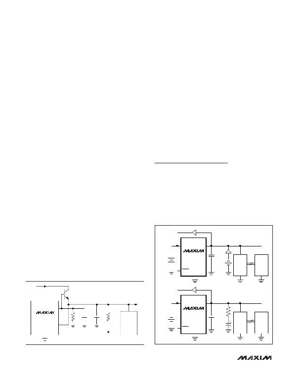
�remotely� sense� the� output� voltage� of� the� device.� Using�
�FB� with� an� external� npn� transistor,� the� current� drive� capa-�
�bility� can� be� increased� according� to� the� following� equa-�
�tion� (Figure� 2):�
�I� OUT(TOTAL)� =� I� OUT� � (� β� +1)�
�The� external� npn� pass� transistor� must� meet� specifica-�
�tions� for� current� gain,� power� dissipation,� and� collector�
�current.� The� beta� influences� the� maximum� output� cur-�
�rent� the� circuit� can� deliver.� The� largest� guaranteed� out-�
�put� current� is� given� by� I� LOAD� (max)� =� 300mA� � beta�
�(min).� The� transistor’s� rated� power� dissipation� must�
�exceed� the� actual� power� dissipated� in� the� transistor.�
�The� power� dissipated� (PD)� equals� the� maximum� load�
�current� (I� LOAD� (max))� times� the� maximum� input-to-out-�
�put� voltage� differential:� PD� =� I� LOAD� (max)� � (V� IN� (max)� -�
�V� OUT� ).� The� rated� transistor� collector� current� must�
�exceed� the� maximum� load� current.�
�Reverse� Leakage� Protection�
�Reverse� OUT� to� IN� Current�
�An� internal� circuit� monitors� the� MAX6469� –MAX6484�
�input� and� output� voltages.� When� the� output� voltage� is�
�greater� than� the� input� voltage,� the� internal� IN-to-OUT�
�pass� transistor� and� parasitic� diode� turn� off.� An� external�
�voltage� applied� to� OUT� does� not� reverse� charge� a� bat-�
�tery� or� power� source� applied� to� IN� (the� leakage� path�
�from� OUT� to� IN� is� 0.01μA� typ).� When� the� output� voltage�
�exceeds� the� input� voltage,� OUT� powers� the� device� and�
�shutdown� must� be� logic� high� (greater� than� 0.7� � V� OUT� ).�
�RESET� asserts� until� IN� exceeds� OUT� and� OUT� is� above�
�the� specified� V� THOUT� threshold� (based� on� the� selected�
�or� adjusted� regulator� OUT� nominal� voltage).�
�OUT-to-GND� current� through� the� LDO� is� 40μA� (typ).� The�
�regulator� output� can� be� held� up� with� an� external� super�
�capacitor� or� backup� battery� at� OUT� until� the� IN� battery� is�
�replaced.� The� RESET� output� is� asserted� while� the� IN� bat-�
�tery� is� removed� to� place� the� system� in� a� low-power�
�mode.� Volatile� memory� content� is� maintained� until� the�
�super� capacitor� or� battery� voltage� drops� below� RAM�
�standby� specifications.� RESET� deasserts� when� the� IN�
�battery� has� been� replaced� and� OUT� exceeds� the�
�desired� reset� threshold.� For� nonrechargeable� backup�
�battery� applications,� place� a� reverse� diode� between�
�OUT� and� the� backup� battery� (to� prevent� battery� charg-�
�ing).� The� external� diode� does� not� affect� the� regulator’s�
�dropout� voltage� because� it� is� not� between� the� LDO� out-�
�put� and� the� processor/memory� V� CC� supply.� The� diode�
�can� be� replaced� with� a� current-limiting� resistor� for�
�rechargeable� backup� battery� applications.�
�Current� Limit�
�The� MAX6469–MAX6484� include� an� internal� current-�
�limit� circuit� that� monitors� and� controls� the� pass� transis-�
�tor’s� gate� voltage,� limiting� the� output� current� to� 450mA�
�(min).� The� output� can� be� shorted� to� ground� indefinitely�
�without� damaging� the� part.�
�Thermal� Shutdown�
�When� the� junction� temperature� (T� J� )� exceeds� +180°C�
�(typ),� the� thermal� sensor� signals� the� shutdown� logic,�
�turning� off� the� pass� transistor� and� allowing� the� IC� to�
�REMOVABLE�
�LITHIUM� ION� OR�
�3-CELL�
�ALKALINE�
�Reverse� OUT� to� Ground� Current�
�IN�
�OUT�
�The� MAX6469–MAX6484� maintain� a� low� OUT-to-GND�
�MAX6469� –�
�3.3� μ� F�
�reverse-current� flow� when� the� IN� power� source� is�
�removed.� When� IN� floats� (input� battery� removed)� and�
�MAX6484�
�3.0V�
�LITHIUM�
�μ� P�
�MEMORY�
�SHDN� is� pulled� up� to� V� OUT� (by� an� external� diode),� the�
�5.0V�
�REMOVABLE�
�LITHIUM� ION� OR�
�SHDN�
�IN�
�1A� TOTAL� CURRENT�
�V� CC� =� 3.3V�
�3-CELL�
�ALKALINE�
�IN�
�OUT�
�OUT�
�MAX6475/MAX6476�
�MAX6483/MAX6484�
�FB�
�330� ?�
�3.3� μ� F�
�0.1� μ� F�
�R� PULLUP�
�μ� P�
�MAX6469� –�
�MAX6484�
�3.3� μ� F�
�SUPERCAP�
�μ� P�
�MEMORY�
�SHDN�
�GND�
�RESET�
�Figure� 2.� High-Current,� External� Transistor� Application�
�Figure� 3.� Battery� Backup�
�10�
�______________________________________________________________________________________�
�相关PDF资料 |
PDF描述 |
|---|---|
| MIC29302BU TR | IC REG LDO ADJ 3A TO263-5 |
| CWR29HH226KCFC | CAP TANT 22UF 15V 10% 2214 |
| VE-2W2-CY-F3 | CONVERTER MOD DC/DC 15V 50W |
| MAX6473TA15AD3+T | IC REG LDO 1.5V/ADJ .3A 8-TDFN |
| CWR29FC686KCGB | CAP TANT 68UF 10V 10% 2711 |
相关代理商/技术参数 |
参数描述 |
|---|---|
| MAX6473TA18BD4+T | 功能描述:低压差稳压器 - LDO RoHS:否 制造商:Texas Instruments 最大输入电压:36 V 输出电压:1.4 V to 20.5 V 回动电压(最大值):307 mV 输出电流:1 A 负载调节:0.3 % 输出端数量: 输出类型:Fixed 最大工作温度:+ 125 C 安装风格:SMD/SMT 封装 / 箱体:VQFN-20 |
| MAX6473TA18BD4-T | 功能描述:低压差稳压器 - LDO RoHS:否 制造商:Texas Instruments 最大输入电压:36 V 输出电压:1.4 V to 20.5 V 回动电压(最大值):307 mV 输出电流:1 A 负载调节:0.3 % 输出端数量: 输出类型:Fixed 最大工作温度:+ 125 C 安装风格:SMD/SMT 封装 / 箱体:VQFN-20 |
| MAX6473TA19AD1+T | 功能描述:低压差稳压器 - LDO RoHS:否 制造商:Texas Instruments 最大输入电压:36 V 输出电压:1.4 V to 20.5 V 回动电压(最大值):307 mV 输出电流:1 A 负载调节:0.3 % 输出端数量: 输出类型:Fixed 最大工作温度:+ 125 C 安装风格:SMD/SMT 封装 / 箱体:VQFN-20 |
| MAX6473TA19AD1-T | 功能描述:低压差稳压器 - LDO RoHS:否 制造商:Texas Instruments 最大输入电压:36 V 输出电压:1.4 V to 20.5 V 回动电压(最大值):307 mV 输出电流:1 A 负载调节:0.3 % 输出端数量: 输出类型:Fixed 最大工作温度:+ 125 C 安装风格:SMD/SMT 封装 / 箱体:VQFN-20 |
| MAX6473TA19AD2+T | 功能描述:低压差稳压器 - LDO RoHS:否 制造商:Texas Instruments 最大输入电压:36 V 输出电压:1.4 V to 20.5 V 回动电压(最大值):307 mV 输出电流:1 A 负载调节:0.3 % 输出端数量: 输出类型:Fixed 最大工作温度:+ 125 C 安装风格:SMD/SMT 封装 / 箱体:VQFN-20 |
发布紧急采购,3分钟左右您将得到回复。