参数资料
| 型号: | MAX6496ATA+T |
| 厂商: | Maxim Integrated Products |
| 文件页数: | 3/16页 |
| 文件大小: | 0K |
| 描述: | IC CTLR PROT SW 8-TDFN |
| 其它有关文件: | Automotive Product Guide |
| 产品培训模块: | Lead (SnPb) Finish for COTS Obsolescence Mitigation Program |
| 标准包装: | 1 |
| 电压 - 工作: | 72V |
| 技术: | 混合技术 |
| 功率(瓦特): | 1.45W |
| 电路数: | 1 |
| 应用: | 通用 |
| 封装/外壳: | 8-WDFN 裸露焊盘 |
| 供应商设备封装: | 8-TDFN-EP(3x3) |
| 包装: | 标准包装 |
| 其它名称: | MAX6496ATA+TDKR |
MAX6495–MAX6499
72V, Overvoltage-Protection Switches/
Limiter Controllers with an External MOSFET
11
Maxim Integrated
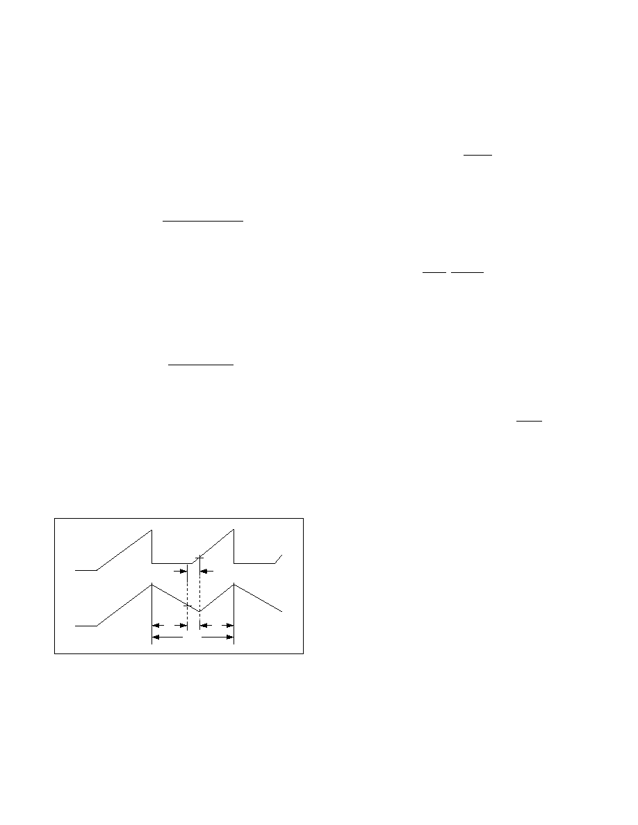
The overvoltage waveform period (tOV)
The power dissipated across the package (PDISS)
During an initial overvoltage occurrence, the discharge
time (Δt1) of COUT, caused by IOUT and IGATEPD. The
discharge time is approximately:
where VOV is the overvoltage threshold, IOUT is the load
current, and IGATEPD is the GATE’s 100mA pulldown
current.
Upon OUT falling below the threshold point, the
MAX6495/MAX6496/MAX6499s’ charge-pump current
must recover and begins recharging the external GATE
voltage. The time needed to recharge GATE from -VD to
the MOSFET’s gate threshold voltage is:
where CISS is the MOSFET’s input capacitance,
VGS(TH) is the MOSFET’s gate threshold voltage, VD is
the internal clamp (from OUTFB to GATE) diode’s for-
ward voltage (1.5V, typ) and IGATE is the charge-pump
current (100A typ).
During Δt2, COUT loses charge through the output load.
The voltage across COUT (ΔV2) decreases until the
MOSFET reaches its VGS(TH) threshold and can be
approximated using the following formula:
Once the MOSFET VGS(TH) is obtained, the slope of the
output-voltage rise is determined by the MOSFET Qg
charge through the internal charge pump with respect
to the drain potential. The new rise time needed to
reach a new overvoltage event can be calculated using
the following formula:
where QGD is the gate-to-drain charge.
The total period of the overvoltage waveform can be
summed up as follows:
ΔtOV = Δt1 + Δt2 + Δt3
The MAX6495/MAX6496/MAX6499 dissipate the most
power during an overvoltage event when IOUT = 0. The
maximum power dissipation can be approximated
using the following equation:
The die-temperature increase is related to
θJC (8.3°C/W
and 8.5°C/W for the MAX6495/MAX6496/MAX6499,
respectively) of the package when mounted correctly
with a strong thermal contact to the circuit board. The
MAX6495/MAX6496/MAX6499 thermal shutdown is
governed by the equation:
TJ = TA + PDISS (
θJC +θCA) < +170°C
Based on these calculations, the parameters of the
MOSFET, the overvoltage threshold, the output load
current, and the output capacitors are external vari-
ables affecting the junction temperature. If these para-
meters are fixed, the junction temperature can also be
affected by increasing Δt3, which is the time the switch
is on. By increasing the capacitance at the GATE pin,
Δt3 increases as it increases the amount of time
required to charge up this additional capacitance
(75A gate current). As a result, ΔtOV increases, there-
by reducing the power dissipated (PDISS).
PV
I
t
DISS
OV
GATEPD
OV
.
=×
×
0 975
1
Δ
t
Q
V
I
GD
GS
OUT
GATE
3
Δ
VI
t
C
OUT
2
=
ΔtC
VV
I
ISS
GS TH
D
GATE
2
()
=
+
ΔtC
V
II
OUT
OV
OUT
GATEPD
1
005
.
(
)
=
×
+
Δt2
Δt1
GATE
OUTFB
ΔtOV
Δt3
Figure 5. MAX6495/MAX6496/MAX6499 Timing
相关PDF资料 |
PDF描述 |
|---|---|
| LTC6240HVHS5#TRMPBF | IC OP AMP SINGLE R-R TSOT23-5 |
| 0034.6921 | FUSE 4A 250V 8.5X8.5 T 4.3 |
| EL5300IU | IC AMP V-FB TRPL 200MHZ 16-QSOP |
| MAX6499ATA+T | IC CTLR PROT SW 8-TDFN |
| LTC6240HVIS5#TRMPBF | IC OP AMP SINGLE R-R TSOT23-5 |
相关代理商/技术参数 |
参数描述 |
|---|---|
| MAX6496EVKIT+ | 功能描述:电源管理IC开发工具 MAX6496 Eval Kit RoHS:否 制造商:Maxim Integrated 产品:Evaluation Kits 类型:Battery Management 工具用于评估:MAX17710GB 输入电压: 输出电压:1.8 V |
| MAX6497ATA+ | 制造商:Maxim Integrated Products 功能描述:OVERVOLT PROT CNTRLR 8TDFN EP - Rail/Tube |
| MAX6497ATA+T | 功能描述:电流和电力监控器、调节器 72V Over V Protect Switch/Limiter RoHS:否 制造商:STMicroelectronics 产品:Current Regulators 电源电压-最大:48 V 电源电压-最小:5.5 V 工作温度范围:- 40 C to + 150 C 安装风格:SMD/SMT 封装 / 箱体:HPSO-8 封装:Reel |
| MAX6498ATA+ | 制造商:Maxim Integrated Products 功能描述:OVERVOLT PROT CNTRLR 8TDFN EP - Rail/Tube |
| MAX6498ATA+T | 功能描述:电流和电力监控器、调节器 72V Over V Protect Switch/Limiter RoHS:否 制造商:STMicroelectronics 产品:Current Regulators 电源电压-最大:48 V 电源电压-最小:5.5 V 工作温度范围:- 40 C to + 150 C 安装风格:SMD/SMT 封装 / 箱体:HPSO-8 封装:Reel |
发布紧急采购,3分钟左右您将得到回复。