- 您现在的位置:买卖IC网 > PDF目录299461 > MAX6629-MAX6632 (Maxim Integrated Products, Inc.) BACKSHELL PDF资料下载
参数资料
| 型号: | MAX6629-MAX6632 |
| 厂商: | Maxim Integrated Products, Inc. |
| 英文描述: | BACKSHELL |
| 中文描述: | 12位注册数字温度传感器的串行接口 |
| 文件页数: | 2/8页 |
| 文件大小: | 152K |
| 代理商: | MAX6629-MAX6632 |
MAX6629–MAX6632
12-Bit + Sign Digital Temperature Sensors
with Serial Interface
2
_______________________________________________________________________________________
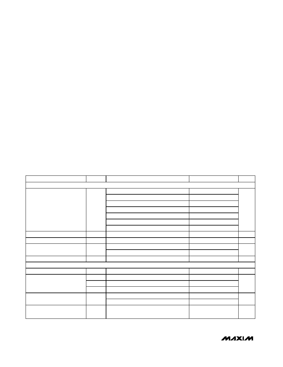
ABSOLUTE MAXIMUM RATINGS
Stresses beyond those listed under “Absolute Maximum Ratings” may cause permanent damage to the device. These are stress ratings only, and functional
operation of the device at these or any other conditions beyond those indicated in the operational sections of the specifications is not implied. Exposure to
absolute maximum rating conditions for extended periods may affect device reliability.
All Voltages Referenced to GND
VCC ...........................................................................-0.3V, +6.0V
SO, SCK, CS ....................................................-0.3V, VCC + 0.3V
SO .......................................................................-1mA to +50mA
Current into Any Pin ............................................................10mA
Continuous Power Dissipation (TA = +70°C)
6-Pin SOT23 (derate 9.10mW/°C above +70°C)..........727mW
Junction Temperature ......................................................+150°C
Operating Temperature Range (Note 1) ...........-55°C to +150°C
Storage Temperature Range .............................-65°C to +150°C
Lead Temperature .............................................................Note 2
ELECTRICAL CHARACTERISTICS
(VCC = +3.0V to +5.5V, TA = -55°C to +125°C, unless otherwise noted. Typical values are at VCC = +3.3V and TA = +25°C.) (Notes 3
and 4)
PARAMETER
SYMBOL
CONDITIONS
MIN
TYP
MAX
UNITS
TEMPERATURE
TA = room temp, VCC = +3.3V
-0.8
±0.2
+0.8
0°C
≤ TA ≤ +70°C, VCC = +3.3V
-1.0
±0.2
+1.0
-20°C
≤ TA ≤ +85°C, VCC = +3.3V
-1.6
+0.3
+1.6
-20°C
≤ TA ≤ +100°C, VCC = +3.3V
-2.3
+0.5
+2.3
°C
-40°C
≤ TA ≤ +125°C, VCC = +3.3V
-3.2
+0.8
+3.2
TA
≥ -55°C, VCC = +3.3V
-1.0
+1.5
+3.5
Accuracy
TA = +150°C, VCC = +3.3V
-5.0
+1.5
+6.5
Power-Supply Sensitivity
PSS
0.2
0.6
°C/V
Resolution
0.0625
°C
MAX6629, MAX6630,
CS high
0.37
0.5
0.65
Time Between Conversion Starts
tSAMPLE
MAX6631, MAX6632,
CS high
5.9
8
10.5
s
Conversion Time
tCONV
180
250
320
ms
POWER SUPPLY
Supply Voltage Range
VCC
3.0
5.5
V
ISD
Shutdown (Note 4), VCC = +0.8V
5
IIDLE
ADC idle (Figure 2),
CS = low
6
20
Supply Current, SCK Idle
ICONV
ADC converting (Figure 2)
360
650
A
MAX6629, MAX6630
200
400
Average Operating Current
ICC
MAX6631, MAX6632
32
50
A
Power-On Reset (POR)
Threshold
VCC falling
1.6
V
Note 1: It is not recommended to operate the device above +125°C for extended periods of time.
Note 2: This device is constructed using a unique set of packaging techniques that impose a limit on the thermal profile the device
can be exposed to during board-level solder attach and rework. This limit permits only the use of the solder profiles
recommended in the industry-standard specification, JEDEC 020A, paragraph 7.6, Table 3 for IR/VPR and Convection
Reflow. Preheating is required. Hand or wave soldering is not allowed.
相关PDF资料 |
PDF描述 |
|---|---|
| MAX6755UK_D_-T | CLAMP |
| MAX6756UK_D_-T | Low-Power, Single/Dual-Voltage Window Detectors |
| MAX6757UT_D_-T | Low-Power, Single/Dual-Voltage Window Detectors |
| MAX702CPA | Power-Supply Monitor with Reset |
| MAX8510EXK31-T | 3.1 V FIXED POSITIVE LDO REGULATOR, 0.17 V DROPOUT, PDSO5 |
相关代理商/技术参数 |
参数描述 |
|---|---|
| MAX6629MTT+ | 制造商:Maxim Integrated Products 功能描述:TEMP SENSOR DGTL 3-WIRE/SPI 6TDFN EP - Rail/Tube |
| MAX6629MTT+T | 功能描述:板上安装温度传感器 12-Bit + Sign Temperature Sensor RoHS:否 制造商:Omron Electronics 输出类型:Digital 配置: 准确性:+/- 1.5 C, +/- 3 C 温度阈值: 数字输出 - 总线接口:2-Wire, I2C, SMBus 电源电压-最大:5.5 V 电源电压-最小:4.5 V 最大工作温度:+ 50 C 最小工作温度:0 C 关闭: 安装风格: 封装 / 箱体: 设备功能:Temperature and Humidity Sensor |
| MAX6629MUT | 制造商:Maxim Integrated Products 功能描述:12-BIT + SIGN DIGITAL TEMPERATURE SENSORS WIT - Rail/Tube |
| MAX6629MUT#G16 | 制造商:Maxim Integrated Products 功能描述:12-BIT + SIGN DIGITAL TEMPERATURE SENSORS WITH SERIAL INTERF - Rail/Tube |
| MAX6629MUT#TG16 | 功能描述:板上安装温度传感器 12-Bit + Sign Temperature Sensor RoHS:否 制造商:Omron Electronics 输出类型:Digital 配置: 准确性:+/- 1.5 C, +/- 3 C 温度阈值: 数字输出 - 总线接口:2-Wire, I2C, SMBus 电源电压-最大:5.5 V 电源电压-最小:4.5 V 最大工作温度:+ 50 C 最小工作温度:0 C 关闭: 安装风格: 封装 / 箱体: 设备功能:Temperature and Humidity Sensor |
发布紧急采购,3分钟左右您将得到回复。