- 您现在的位置:买卖IC网 > PDF目录13341 > MAX6888OETE+T (Maxim Integrated Products)IC SUPERVISOR QUAD 16-TQFN PDF资料下载
参数资料
| 型号: | MAX6888OETE+T |
| 厂商: | Maxim Integrated Products |
| 文件页数: | 5/13页 |
| 文件大小: | 0K |
| 描述: | IC SUPERVISOR QUAD 16-TQFN |
| 产品培训模块: | Lead (SnPb) Finish for COTS Obsolescence Mitigation Program |
| 标准包装: | 2,500 |
| 类型: | 多压监控器 |
| 监视电压数目: | 4 |
| 输出: | 开路漏极或开路集电极 |
| 复位: | 低有效 |
| 复位超时: | 最小为 180 ms |
| 电压 - 阀值: | 2.5V,3.3V,可调,可调 |
| 工作温度: | -40°C ~ 85°C |
| 安装类型: | 表面贴装 |
| 封装/外壳: | 16-WQFN 裸露焊盘 |
| 供应商设备封装: | 16-TQFN-EP(5x5) |
| 包装: | 带卷 (TR) |
�� �
�
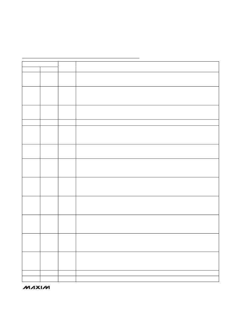
�Hex/Quad,� Power-Supply� Supervisory� Circuits�
�Pin� Description� (continued)�
�PIN�
�MAX6887� MAX6888�
�NAME�
�FUNCTION�
�Manual� Reset� Input.� Pull� MR� low� to� assert� RESET� .� Connect� MR� to� WDO� to� generate� resets�
�5�
�5�
�MR�
�when� the� watchdog� timer� expires.� Leave� MR� unconnected� or� connect� to� DBP� if� unused.� MR� is�
�internally� pulled� up� to� BP� through� a� 10μA� current� source.�
�Margin� Input.� When� MARGIN� is� pulled� low,� RESET� is� held� in� its� existing� state� independent� of�
�6�
�6�
�MARGIN�
�subsequent� changes� in� monitored� input� voltages� or� the� watchdog� timer� expiration.� MARGIN� is�
�internally� pulled� up� to� BP� through� a� 10μA� current� source.� Leave� MARGIN� unconnected� or�
�connect� to� BP� if� unused.� MARGIN� overrides� MR� if� both� are� asserted� at� the� same� time.�
�Watchdog� Timer� Input.� Logic� input� for� the� watchdog� timer� function.� If� WDI� is� not� strobed� with� a�
�7�
�7�
�WDI�
�valid� low-to-high� or� high-to-low� transition� within� the� selected� watchdog� timeout� period,� WDO�
�asserts.� WDI� is� internally� pulled� down� to� GND� through� a� 10μA� current� sink.�
�8�
�8�
�I.C.�
�Internal� Connection.� Leave� unconnected.�
�Internal� Power-Supply� Voltage.� Bypass� V� CC� to� GND� with� a� 1μF� ceramic� capacitor� as� close� to�
�9�
�9�
�V� CC�
�the� device� as� possible.� V� CC� supplies� power� to� the� internal� circuitry.� V� CC� is� internally� powered�
�from� the� highest� of� the� monitored� IN1–IN4� voltages.� Do� not� use� V� CC� to� supply� power� to� external�
�circuitry.� To� externally� supply� V� CC� ,� see� the� Powering� the� MAX6887/MAX6888� section.�
�Bypass� Voltage.� The� internally� generated� voltage� at� BP� supplies� power� to� internal� logic� and�
�10�
�10�
�BP�
�output� RESET� .� Connect� a� 1μF� capacitor� from� BP� to� GND� as� close� to� the� device� as� possible.� Do�
�not� use� BP� to� supply� power� to� external� circuitry.�
�Input� Voltage� Detector� 6.� IN6� monitors� both� undervoltage� and� overvoltage� conditions.� See� the�
�11�
�—�
�IN6�
�thresholds� options� (Tables� 1� and� 2)� for� available� thresholds.� IN6� cannot� power� the� device.� For�
�improved� noise� immunity,� bypass� IN6� to� GND� with� a� 0.1μF� capacitor� installed� as� close� to� the�
�device� as� possible.�
�Input� Voltage� Detector� 5.� IN5� monitors� both� undervoltage� and� overvoltage� conditions.� See� the�
�12�
�—�
�IN5�
�thresholds� options� (Tables� 1� and� 2)� for� available� thresholds.� IN5� cannot� power� the� device.� For�
�improved� noise� immunity,� bypass� IN5� to� GND� with� a� 0.1μF� capacitor� installed� as� close� to� the�
�device� as� possible.�
�Input� Voltage� Detector� 4.� IN4� monitors� both� undervoltage� and� overvoltage� conditions.� See� the�
�13�
�13�
�IN4�
�thresholds� options� (Tables� 1� and� 2)� for� available� thresholds.� Power� the� device� through� IN1–IN4�
�or� V� CC� (see� the� Powering� the� MAX6887/MAX6888� section).� For� improved� noise� immunity,�
�bypass� IN4� to� GND� with� a� 0.1μF� capacitor� installed� as� close� to� the� device� as� possible.�
�Input� Voltage� Detector� 3.� IN3� monitors� both� undervoltage� and� overvoltage� conditions.� See� the�
�14�
�14�
�IN3�
�thresholds� options� (Tables� 1� and� 2)� for� available� thresholds.� Power� the� device� through� IN1–IN4�
�or� V� CC� (see� the� Powering� the� MAX6887/MAX6888� section).� For� improved� noise� immunity,�
�bypass� IN3� to� GND� with� a� 0.1μF� capacitor� installed� as� close� to� the� device� as� possible.�
�Input� Voltage� Detector� 2.� IN2� monitors� both� undervoltage� and� overvoltage� conditions.� See� the�
�15�
�15�
�IN2�
�thresholds� options� (Tables� 1� and� 2)� for� available� thresholds.� Power� the� device� through� IN1–IN4�
�or� V� CC� (see� the� Powering� the� MAX6887/MAX6888� section).� For� improved� noise� immunity,�
�bypass� IN2� to� GND� with� a� 0.1μF� capacitor� installed� as� close� to� the� device� as� possible.�
�Input� Voltage� Detector� 1.� IN1� monitors� both� undervoltage� and� overvoltage� conditions.� See� the�
�16�
�16�
�IN1�
�thresholds� options� (Tables� 1� and� 2)� for� available� thresholds.� Power� the� device� through� IN1–IN4�
�or� V� CC� (see� the� Powering� the� MAX6887/MAX6888� section).� For� improved� noise� immunity,�
�bypass� IN1� to� GND� with� a� 0.1μF� capacitor� installed� as� close� to� the� device� as� possible.�
�—�
�—�
�11,� 12�
�—�
�N.C.�
�EP�
�No� Connection.� Not� internally� connected.�
�Exposed� Paddle.� Internally� connected� to� GND.� Connect� EP� to� GND� or� leave� unconnected.�
�_______________________________________________________________________________________�
�5�
�相关PDF资料 |
PDF描述 |
|---|---|
| EMM15DTAH | CONN EDGECARD 30POS R/A .156 SLD |
| V375B15C200BL3 | CONVERTER MOD DC/DC 15V 200W |
| AP7312-3333W6-7 | IC REG LDO 3.3V .15A SOT26 |
| VI-2TF-EX-F2 | CONVERTER MOD DC/DC 72V 75W |
| ISL6410IU-T5K | IC REG BUCK SYNC 0.6A 10MSOP |
相关代理商/技术参数 |
参数描述 |
|---|---|
| MAX6888PETE | 功能描述:监控电路 RoHS:否 制造商:STMicroelectronics 监测电压数: 监测电压: 欠电压阈值: 过电压阈值: 输出类型:Active Low, Open Drain 人工复位:Resettable 监视器:No Watchdog 电池备用开关:No Backup 上电复位延迟(典型值):10 s 电源电压-最大:5.5 V 最大工作温度:+ 85 C 安装风格:SMD/SMT 封装 / 箱体:UDFN-6 封装:Reel |
| MAX6888PETE+ | 功能描述:监控电路 Quad Power-Supply Supervisor RoHS:否 制造商:STMicroelectronics 监测电压数: 监测电压: 欠电压阈值: 过电压阈值: 输出类型:Active Low, Open Drain 人工复位:Resettable 监视器:No Watchdog 电池备用开关:No Backup 上电复位延迟(典型值):10 s 电源电压-最大:5.5 V 最大工作温度:+ 85 C 安装风格:SMD/SMT 封装 / 箱体:UDFN-6 封装:Reel |
| MAX6888PETE+T | 功能描述:监控电路 Quad Power-Supply Supervisor RoHS:否 制造商:STMicroelectronics 监测电压数: 监测电压: 欠电压阈值: 过电压阈值: 输出类型:Active Low, Open Drain 人工复位:Resettable 监视器:No Watchdog 电池备用开关:No Backup 上电复位延迟(典型值):10 s 电源电压-最大:5.5 V 最大工作温度:+ 85 C 安装风格:SMD/SMT 封装 / 箱体:UDFN-6 封装:Reel |
| MAX6888PETE-T | 功能描述:监控电路 RoHS:否 制造商:STMicroelectronics 监测电压数: 监测电压: 欠电压阈值: 过电压阈值: 输出类型:Active Low, Open Drain 人工复位:Resettable 监视器:No Watchdog 电池备用开关:No Backup 上电复位延迟(典型值):10 s 电源电压-最大:5.5 V 最大工作温度:+ 85 C 安装风格:SMD/SMT 封装 / 箱体:UDFN-6 封装:Reel |
| MAX6888QETE | 功能描述:监控电路 RoHS:否 制造商:STMicroelectronics 监测电压数: 监测电压: 欠电压阈值: 过电压阈值: 输出类型:Active Low, Open Drain 人工复位:Resettable 监视器:No Watchdog 电池备用开关:No Backup 上电复位延迟(典型值):10 s 电源电压-最大:5.5 V 最大工作温度:+ 85 C 安装风格:SMD/SMT 封装 / 箱体:UDFN-6 封装:Reel |
发布紧急采购,3分钟左右您将得到回复。