- 您现在的位置:买卖IC网 > PDF目录20727 > MAX688CUA+ (Maxim Integrated)IC REG LDO 3.3V 1A 8-UMAX PDF资料下载
参数资料
| 型号: | MAX688CUA+ |
| 厂商: | Maxim Integrated |
| 文件页数: | 7/12页 |
| 文件大小: | 0K |
| 描述: | IC REG LDO 3.3V 1A 8-UMAX |
| 产品培训模块: | Lead (SnPb) Finish for COTS Obsolescence Mitigation Program |
| 标准包装: | 50 |
| 稳压器拓扑结构: | 正,固定式 |
| 输出电压: | 3.3V |
| 输入电压: | 最高 11V |
| 电压 - 压降(标准): | 0.04V @ 200mA |
| 稳压器数量: | 1 |
| 电流 - 输出: | 1A |
| 工作温度: | 0°C ~ 70°C |
| 安装类型: | 表面贴装 |
| 封装/外壳: | 8-TSSOP,8-MSOP(0.118",3.00mm 宽) |
| 供应商设备封装: | 8-uMAX |
| 包装: | 管件 |
�� �
�
�High-Accuracy,� Low-Dropout�
�Linear� Regulators�
�shuts� down.� Once� the� MAX687� is� shut� down,� it� can�
�only� be� turned� on� again� when� (a)� the� ON� pin� is� pulsed�
�high,� and� (b)� the� conditions� that� triggered� shutdown�
�have� changed� (e.g.,� the� load� has� been� reduced� or� the�
�input� voltage� has� increased).� In� order� for� the� MAX687�
�to� latch� into� its� on� state,� the� ON� pulse� must� remain� high�
�until� the� output� voltage� has� risen� above� the� shutdown�
�threshold.� The� internal� shutdown� can� be� used� to� pre-�
�vent� deep� discharge� of� a� battery,� for� example,� to� pro-�
�vide� “self� backup� ”� of� CMOS� RAM� or� to� protect� the�
�battery� itself.�
�The� RC� circuit� attached� to� the� ON� input� in� Figure� 1�
�achieves� automatic� start-up� at� power-on� by� delivering� a�
�brief� pulse� whenever� the� input� voltage� is� suddenly�
�applied.� This� circuit� is� not� suitable� for� applications�
�where� the� input� voltage� rises� slowly.� The� RC� values�
�should� be� chosen� to� keep� ON� high� until� the� output� rises�
�above� about� 3.13V.� The� values� shown� in� Figure� 1� for�
�C4� and� R1� (0.1μF� and� 10k� ?� )� are� suitable� for� most�
�applications.� To� ensure� start-up� when� the� input� voltage�
�is� very� close� to� the� circuit’s� dropout� voltage,� when� the�
�circuit� is� used� to� drive� a� very� large� capacitive� load,� or�
�for� high-power� circuits� (I� LOAD� >� 3A),� increase� the� value�
�of� R1� to� increase� the� ON� pulse� width.�
�The� 3.3V� MAX688� and� the� 3.0V� MAX689� incorporate�
�the� same� PFO� warning� whenever� V� OUT� droops.�
�However,� the� MAX688/MAX689� do� not� automatically�
�shut� down� when� the� output� voltage� drops� even� further.�
�Instead,� the� SHDN� input� controls� external� shutdown.�
�As� SHDN� is� pulled� low,� the� chip� first� enters� a� low-cur-�
�rent� standby� state� (<25μA).� The� threshold� at� which�
�standby� mode� is� entered� is� precisely� controlled� (±2%)�
�so� the� output� can� be� turned� off� at� a� well-defined� point.�
�70mV� of� hysteresis� between� the� standby� and� on� states�
�prevents� chatter� between� the� two� modes.� The� voltage�
�applied� to� the� SHDN� pin� can� be� derived� from� a� resis-�
�tive� divider� from� V� IN� .� When� V� SHDN� is� less� than� 1.2V,�
�the� output� is� off.� The� device� is� fully� shut� down� (<1μA)�
�when� SHDN� is� pulle� d� below� 200mV.� SHDN� is� not�
�latched,� and� as� SHDN� is� raised,� the� MAX688/MAX689�
�exit� shutdown� and� enter� the� standby� mode.� At� the�
�higher� SHDN� threshold,� the� output� is� turned� on.�
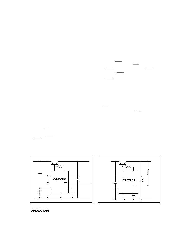
�Figure� 1� shows� a� typical� circuit� for� the� MAX687,� and�
�Figure� 2� shows� the� same� circuit� configured� for� the�
�MAX688/MAX689.�
�The� accuracy� of� the� output� current� limit� depends� on�
�accurate� knowledge� of� the� PNP� pass� transistor’s� cur-�
�rent� gain� (h� FE� ).� With� R� B� =� 12� ?� ,� BLIM� limits� base� cur-�
�rent� to� 6mA� (I� BASE� =� 0.1V� /� (R� B� +� 5� ?� )).� See� Base-�
�Current� Limiting� section.�
�The� PFO� comparators� on� all� three� devices,� and� the� internal�
�shutdown� comparator� on� the� MAX687,� reject� high-speed�
�spikes� (<100μs).� This� reduces� the� PFO� output’s� noise� sen-�
�sitivity,� and� stops� the� MAX687� from� being� shut� down� inad-�
�vertently� when� there� is� noise� on� the� input� supply.�
�_______________Transistor� Selection�
�Specifications�
�The� PNP� pass� transistor� must� meet� specifications� for�
�?� current� gain,�
�?� power� dissipation,� and�
�?� collector� current.�
�The� h� FE� influences� the� maximum� output� current� the� cir-�
�cuit� can� deliver.� The� largest� guaranteed� output� current�
�+5V� INPUT�
�Q1� FZT749�
�3.3V� @� 500mA�
�+5V� INPUT�
�Q1� FZT749�
�3.3V/� 3.0V� @� 500mA�
�C4�
�0.1� μ� F�
�R� B� 12� ?�
�BASE�
�IN�
�BLIM�
�OUT�
�BASE�
�IN�
�R� B� 12� ?�
�BLIM�
�OUT�
�R2�
�100k�
�C1�
�2.2� μ� F�
�ON�
�MAX687�
�PFO�
�CC�
�C2�
�68� μ� F�
�C3�
�POWER� FAIL�
�C1�
�2.2� μ� F�
�ON� /� OFF�
�SHDN�
�MAX688�
�MAX689�
�PFO�
�C2�
�68� μ� F�
�POWER� FAIL�
�GND�
�R1�
�10k� ?�
�GND�
�10nF�
�GND�
�CC�
�C3�
�10nF�
�ON� CAN� BE� DRIVEN� DIRECTLY� FROM� LOGIC� WHEN� R1� AND� C4� ARE� NOT� USED.�
�Figure� 1.� MAX687� Operating� Circuit�
�GND�
�Figure� 2.� MAX688/MAX689� Operating� Circuit�
�_______________________________________________________________________________________�
�7�
�相关PDF资料 |
PDF描述 |
|---|---|
| HMC31DRYN-S734 | CONN EDGECARD 62POS DIP .100 SLD |
| V150B28C250BL | CONVERTER MOD DC/DC 28V 250W |
| AISC-0603-R0033J-T | INDUCTOR WW CERAM 3.3NH 0603 |
| MAX8866REUA+ | IC REG LDO 2.8V/ADJ .1A 8UMAX |
| EEC17DREH-S13 | CONN EDGECARD 34POS .100 EXTEND |
相关代理商/技术参数 |
参数描述 |
|---|---|
| MAX688CUA+ | 功能描述:低压差稳压器 - LDO High-Accuracy LDO RoHS:否 制造商:Texas Instruments 最大输入电压:36 V 输出电压:1.4 V to 20.5 V 回动电压(最大值):307 mV 输出电流:1 A 负载调节:0.3 % 输出端数量: 输出类型:Fixed 最大工作温度:+ 125 C 安装风格:SMD/SMT 封装 / 箱体:VQFN-20 |
| MAX688CUA+T | 功能描述:低压差稳压器 - LDO High-Accuracy LDO RoHS:否 制造商:Texas Instruments 最大输入电压:36 V 输出电压:1.4 V to 20.5 V 回动电压(最大值):307 mV 输出电流:1 A 负载调节:0.3 % 输出端数量: 输出类型:Fixed 最大工作温度:+ 125 C 安装风格:SMD/SMT 封装 / 箱体:VQFN-20 |
| MAX688CUAT | 制造商:MAXIM 功能描述:* |
| MAX688CUA-T | 功能描述:低压差稳压器 - LDO High-Accuracy LDO RoHS:否 制造商:Texas Instruments 最大输入电压:36 V 输出电压:1.4 V to 20.5 V 回动电压(最大值):307 mV 输出电流:1 A 负载调节:0.3 % 输出端数量: 输出类型:Fixed 最大工作温度:+ 125 C 安装风格:SMD/SMT 封装 / 箱体:VQFN-20 |
| MAX688EPA | 功能描述:低压差稳压器 - LDO RoHS:否 制造商:Texas Instruments 最大输入电压:36 V 输出电压:1.4 V to 20.5 V 回动电压(最大值):307 mV 输出电流:1 A 负载调节:0.3 % 输出端数量: 输出类型:Fixed 最大工作温度:+ 125 C 安装风格:SMD/SMT 封装 / 箱体:VQFN-20 |
发布紧急采购,3分钟左右您将得到回复。