- 您现在的位置:买卖IC网 > PDF目录3774 > MAX7314AEG+ (Maxim Integrated Products)IC I/O EXPANDER I2C 16B 24QSOP PDF资料下载
参数资料
| 型号: | MAX7314AEG+ |
| 厂商: | Maxim Integrated Products |
| 文件页数: | 2/25页 |
| 文件大小: | 0K |
| 描述: | IC I/O EXPANDER I2C 16B 24QSOP |
| 产品培训模块: | Lead (SnPb) Finish for COTS Obsolescence Mitigation Program |
| 标准包装: | 50 |
| 接口: | I²C |
| 输入/输出数: | 18 |
| 中断输出: | 是 |
| 频率 - 时钟: | 400kHz |
| 电源电压: | 2 V ~ 3.6 V |
| 工作温度: | -40°C ~ 125°C |
| 安装类型: | 表面贴装 |
| 封装/外壳: | 24-SSOP(0.154",3.90mm 宽) |
| 供应商设备封装: | 24-QSOP |
| 包装: | 管件 |
MAX7314
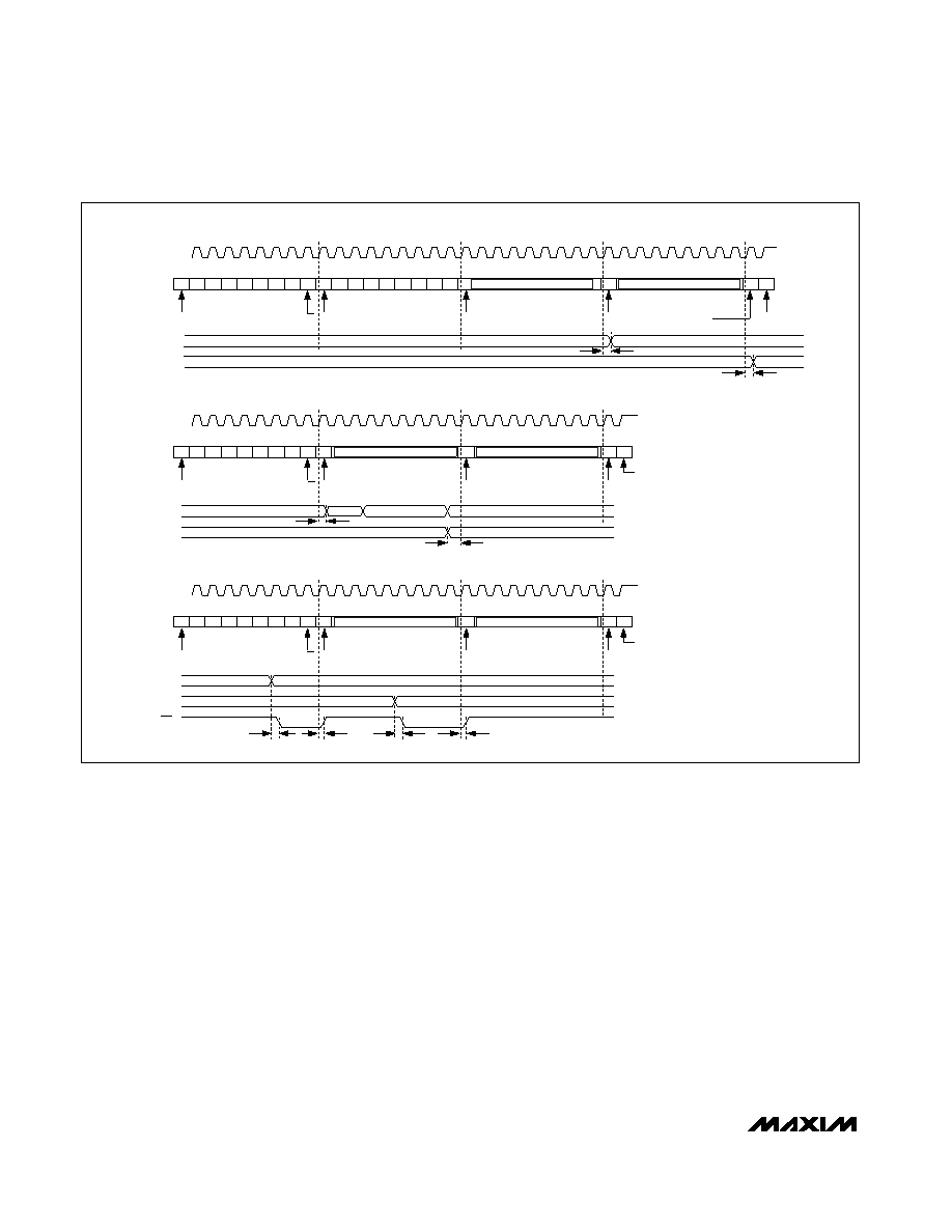
Message Format for Reading
The MAX7314 is read using the MAX7314’s internally
stored command byte as an address pointer the same
way the stored command byte is used as an address
pointer for a write. The pointer autoincrements after
each data byte is read using the same rules as for a
write (Table 2). Thus, a read is initiated by first configur-
ing the MAX7314’s command byte by performing a
write (Figure 7). The master can now read n consecu-
tive bytes from the MAX7314 with the first data byte
being read from the register addressed by the initial-
ized command byte. When performing read-after-write
verification, remember to reset the command byte’s
address because the stored command byte address
has been autoincremented after the write (Table 2). A
diagram of a read from the input ports registers is
shown in Figure 10 reflecting the states of the ports.
Operation with Multiple Masters
If the MAX7314 is operated on a 2-wire interface with
multiple masters, a master reading the MAX7314 should
use a repeated start between the write, which sets the
MAX7314’s address pointer, and the read(s) that takes
the data from the location(s) (Table 2). This is because it
is possible for master 2 to take over the bus after master
1 has set up the MAX7314’s address pointer but before
master 1 has read the data. If master 2 subsequently
changes the MAX7314’s address pointer, then master
1’s delayed read can be from an unexpected location.
Command Address Autoincrementing
The command address stored in the MAX7314 circu-
lates around grouped register functions after each data
byte is written or read (Table 2).
18-Port GPIO with LED Intensity Control,
Interrupt, and Hot-Insertion Protection
10
______________________________________________________________________________________
Figure 10. Read, Write, and Interrupt Timing Diagrams
SLAVE ADDRESS
1
23
4567
89
S A6 A5 A4 A3 A2 A1 A00
A
0
00
COMMAND BYTE
1A
A
P
START CONDITION
ACKNOWLEDGE FROM SLAVE
STOP
CONDITION
P7–P0
P15– P8
DATA1 VALID
DATA2 VALID
SLAVE ADDRESS
1
23
4567
89
S A6A5A4A3A2A1A0
1
A
COMMAND BYTE
ANA
START CONDITION
ACKNOWLEDGE FROM SLAVE
ACKNOWLEDGE FROM MASTER
P7–P0
P15–P8
STOP CONDITION
P
NO ACKNOWLEDGE FROM
MASTER
DATA2
DATA4
DATA3
tDV
SLAVE ADDRESS
1
23
4567
89
S A6A5A4A3A2A1A0 1
A
COMMAND BYTE
ANA
START CONDITION
ACKNOWLEDGE FROM SLAVE
ACKNOWLEDGE FROM MASTER
P7–P0
P15–P8
STOP CONDITION
P
NO ACKNOWLEDGE FROM
MASTER
DATA1
DATA2
DATA3
DATA4
DATA6
DATA5
tDH
tDS
DATA1
tIV
tIR
tIV
SCL
SDA
SCL
SDA
SCL
SDA
WRITE TO OUTPUT PORTS REGISTERS (BLINK PHASE 0 REGISTERS/BLINK PHASE 1 REGISTERS)
READ FROM INPUT PORTS REGISTERS
INTERRUPT VALID/RESET
R/W
MSB
LSB
DATA1
MSB
LSB
DATA1
MSB
LSB
DATA2
MSB
LSB
DATA4
MSB
LSB
DATA6
MSB
LSB
DATA2
R/W
INT
相关PDF资料 |
PDF描述 |
|---|---|
| MAX7313AEG+ | IC I/O EXPANDER I2C 16B 24QSOP |
| MAX7318ATG+ | IC I/O EXPANDER I2C 16B 24TQFN |
| MAX7312AAG+ | IC I/O EXPANDER I2C 16B 24SSOP |
| MAX7313ATG+ | IC I/O EXPANDER I2C 16B 24TQFN |
| MAX7318AUG+ | IC I/O EXPANDER I2C 16B 24TSSOP |
相关代理商/技术参数 |
参数描述 |
|---|---|
| MAX7314AEG+ | 功能描述:外围驱动器与原件 - PCI 18-Port GPIO RoHS:否 制造商:PLX Technology 工作电源电压: 最大工作温度: 安装风格:SMD/SMT 封装 / 箱体:FCBGA-1156 封装:Tray |
| MAX7314AEG+T | 功能描述:外围驱动器与原件 - PCI 18-Port GPIO RoHS:否 制造商:PLX Technology 工作电源电压: 最大工作温度: 安装风格:SMD/SMT 封装 / 箱体:FCBGA-1156 封装:Tray |
| MAX7314AEG-T | 功能描述:外围驱动器与原件 - PCI 18-Port GPIO RoHS:否 制造商:PLX Technology 工作电源电压: 最大工作温度: 安装风格:SMD/SMT 封装 / 箱体:FCBGA-1156 封装:Tray |
| MAX7314ATG | 功能描述:外围驱动器与原件 - PCI RoHS:否 制造商:PLX Technology 工作电源电压: 最大工作温度: 安装风格:SMD/SMT 封装 / 箱体:FCBGA-1156 封装:Tray |
| MAX7314ATG+ | 功能描述:外围驱动器与原件 - PCI 18-Port GPIO RoHS:否 制造商:PLX Technology 工作电源电压: 最大工作温度: 安装风格:SMD/SMT 封装 / 箱体:FCBGA-1156 封装:Tray |
发布紧急采购,3分钟左右您将得到回复。