- 您现在的位置:买卖IC网 > PDF目录1945 > MAX7320ATE+T (Maxim Integrated Products)IC I/O EXPANDER I2C 8B 16TQFN-EP PDF资料下载
参数资料
| 型号: | MAX7320ATE+T |
| 厂商: | Maxim Integrated Products |
| 文件页数: | 7/14页 |
| 文件大小: | 0K |
| 描述: | IC I/O EXPANDER I2C 8B 16TQFN-EP |
| 产品培训模块: | Lead (SnPb) Finish for COTS Obsolescence Mitigation Program |
| 标准包装: | 2,500 |
| 接口: | I²C |
| 输入/输出数: | 8 |
| 中断输出: | 无 |
| 频率 - 时钟: | 400kHz |
| 电源电压: | 1.71 V ~ 5.5 V |
| 工作温度: | -40°C ~ 125°C |
| 安装类型: | 表面贴装 |
| 封装/外壳: | 16-WFQFN 裸露焊盘 |
| 供应商设备封装: | 16-TQFN-EP(3x3) |
| 包装: | 带卷 (TR) |
| 包括: | POR |
MAX7320
I2C Port Expander with Eight Push-Pull Outputs
2
_______________________________________________________________________________________
ABSOLUTE MAXIMUM RATINGS
Stresses beyond those listed under “Absolute Maximum Ratings” may cause permanent damage to the device. These are stress ratings only, and functional
operation of the device at these or any other conditions beyond those indicated in the operational sections of the specifications is not implied. Exposure to
absolute maximum rating conditions for extended periods may affect device reliability.
(All voltages referenced to GND.)
Supply Voltage V+....................................................-0.3V to +6V
SCL, SDA, AD0, AD2, RST .......................................-0.3V to +6V
O0–07...............................................................0.3V to V+ + 0.3V
00–07 Output Current .......................................................±25mA
SDA Input Current.............................................................. 10mA
Total V+ Current..................................................................50mA
Total GND Current ...........................................................100mA
Continuous Power Dissipation (TA = +70°C)
16-Pin QSOP (derate 8.3mW/°C over +70°C)..............667mW
16-Pin Thin QFN (derate 15.6mW/°C over +70°C) ....1250mW
Operating Temperature Range .........................-40°C to +125°C
Junction Temperature ......................................................+150°C
Storage Temperature Range .............................-65°C to +150°C
Lead Temperature (soldering, 10s) .................................+300°C
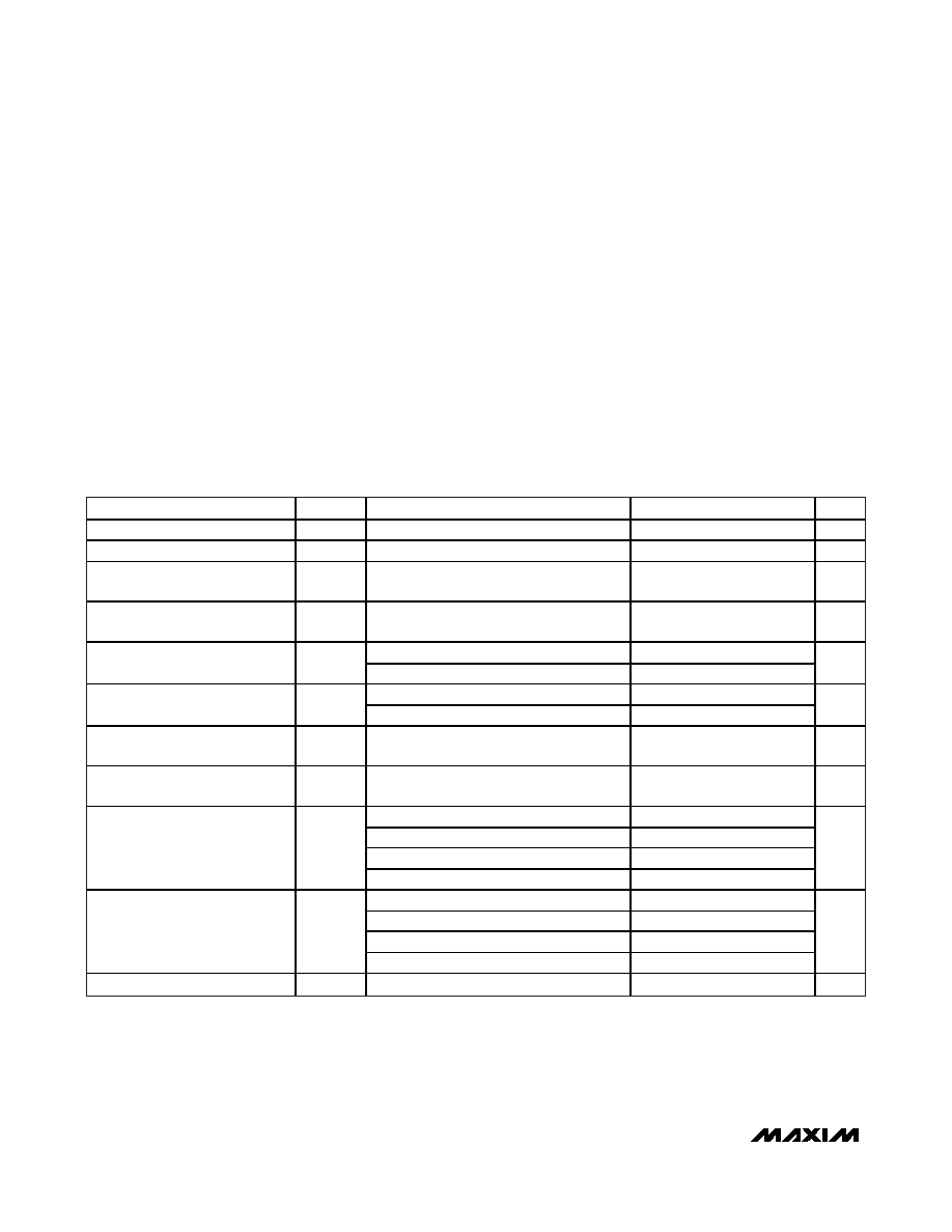
ELECTRICAL CHARACTERISTICS
(V+ = +1.71V to +5.5V, TA = -40°C to +125°C, unless otherwise noted. Typical values are at V+ = +3.3V, TA = +25°C.) (Note 1)
PARAMETER
SYMBOL
CONDITIONS
MIN
TYP
MAX
UNITS
Operating Supply Voltage
V+
1.71
5.50
V
Power-On Reset Voltage
VPOR
1.6
V
Standby Current Voltage
(Interface Idle)
ISTB
SCL and SDA and other digital inputs at V+
0.6
1.5
A
Supply Current
(Interface Running)
I+
fSCL = 400kHz; other digital inputs at V+
23
55
A
V+ < 1.8V
0.8 x V+
Input High-Voltage
SDA, SCL, AD0, AD2, RST
VIH
V+
≥ 1.8V
0.7 x V+
V
V+ < 1.8V
0.2 x V+
Input Low-Voltage
SDA, SCL, AD0, AD2, RST
VIL
V+
≥ 1.8V
0.3 x V+
V
Input Leakage Current
SDA, SCL, AD0, AD2, RST
IIH, IIL
SDA, SCL, AD0, AD2, RST, O0–O7 at V+ or
GND
-0.2
+0.2
A
Input Capacitance
SDA, SCL, AD0, AD2, RST
10
pF
V+ = +1.71V, ISINK = 1mA
120
240
V+ = +2.5V, ISINK = 2mA
140
280
V+ = +3.3V, ISINK = 3mA
170
310
Output Low Voltage
O0–O7
VOL
V+ = +5V, ISINK = 5mA
220
380
mV
V+ = +1.71V, ISOURCE = 1mA
V+ - 250
V+ - 130
V+ = +2.5V, ISOURCE = 2mA
V+ - 350 V+ - 200
V+ = +3.3V, ISOURCE = 3mA
V+ - 290 V+ - 150
Output High Voltage
O0–O7
VOH
V+ = +5V, ISOURCE = 5mA
V+ - 380
V+ - 230
mV
Output Low Voltage SDA
VOLSDA
ISINK = 6mA
250
mV
相关PDF资料 |
PDF描述 |
|---|---|
| MAX7321AEE+ | IC I/O EXPANDER I2C 8B 16QSOP |
| MAX7322ATE+T | IC I/O EXPANDER I2C 4B 16TQFN-EP |
| MAX7323ATE+T | IC I/O EXPANDER I2C 4B 16TQFN-EP |
| MAX7324ATG+ | IC I/O EXPANDER I2C 8B 24TQFN-EP |
| MAX7325AEG+T | IC I/O EXPANDER I2C 8B 24QSOP |
相关代理商/技术参数 |
参数描述 |
|---|---|
| MAX7320EVKIT+ | 功能描述:界面开发工具 Evaluation Kit for the MAX7320 RoHS:否 制造商:Bourns 产品:Evaluation Boards 类型:RS-485 工具用于评估:ADM3485E 接口类型:RS-485 工作电源电压:3.3 V |
| MAX7321 | 制造商:MAXIM 制造商全称:Maxim Integrated Products 功能描述:I2C Port Expander with 4 Push-Pull Outputs |
| MAX7321AAP | 制造商:MAXIM 制造商全称:Maxim Integrated Products 功能描述:I2C Port Expander with 8 Open-Drain I/Os |
| MAX7321AEE | 功能描述:接口-I/O扩展器 RoHS:否 制造商:NXP Semiconductors 逻辑系列: 输入/输出端数量: 最大工作频率:100 kHz 工作电源电压:1.65 V to 5.5 V 工作温度范围:- 40 C to + 85 C 安装风格:SMD/SMT 封装 / 箱体:HVQFN-16 封装:Reel |
| MAX7321AEE+ | 功能描述:接口-I/O扩展器 I2C Port Expander w/8 Open-Drain I/Os RoHS:否 制造商:NXP Semiconductors 逻辑系列: 输入/输出端数量: 最大工作频率:100 kHz 工作电源电压:1.65 V to 5.5 V 工作温度范围:- 40 C to + 85 C 安装风格:SMD/SMT 封装 / 箱体:HVQFN-16 封装:Reel |
发布紧急采购,3分钟左右您将得到回复。