- 您现在的位置:买卖IC网 > PDF目录3772 > MAX7326ATG+ (Maxim Integrated Products)IC I/O EXPANDER I2C 16B 24TQFN PDF资料下载
参数资料
| 型号: | MAX7326ATG+ |
| 厂商: | Maxim Integrated Products |
| 文件页数: | 18/20页 |
| 文件大小: | 0K |
| 描述: | IC I/O EXPANDER I2C 16B 24TQFN |
| 产品培训模块: | Lead (SnPb) Finish for COTS Obsolescence Mitigation Program |
| 标准包装: | 75 |
| 接口: | I²C |
| 输入/输出数: | 16 |
| 中断输出: | 是 |
| 频率 - 时钟: | 400kHz |
| 电源电压: | 1.71 V ~ 5.5 V |
| 工作温度: | -40°C ~ 125°C |
| 安装类型: | 表面贴装 |
| 封装/外壳: | 24-WFQFN 裸露焊盘 |
| 供应商设备封装: | 24-TQFN-EP(4x4) |
| 包装: | 管件 |
| 包括: | POR |
MAX7326
I2C Port Expander with 12 Push-Pull Outputs
and 4 Inputs
_______________________________________________________________________________________
7
When the MAX7326 is read through the serial interface,
the actual logic levels at the ports are read back.
The four input ports offer latching transition detection
functionality. All input ports are continuously monitored
for changes. An input change sets 1 of 4 flag bits that
identify the changed input(s). All flags are cleared upon
a subsequent read or write transaction to the MAX7326.
A latching interrupt output, INT, is programmed to flag
input data changes on the four input ports through an
interrupt mask register. By default, data changes on
any input port force INT to a logic-low. The interrupt out-
put INT and all transition flags are deasserted when the
MAX7326 is next accessed through the serial interface.
Internal pullup resistors to V+ are selected by the
address select inputs, AD0 and AD2. Pullups are
enabled on the input ports in groups of two (see Table 2).
Initial Power-Up
On power-up, the transition detection logic is reset, and
INT is deasserted. The interrupt mask register is set to
0x3C, enabling the interrupt output for transitions on all
four input ports. The transition flags are cleared to indi-
cate no data changes. The power-up default states of
the 12 push-pull outputs are set according to the I2C
slave address selection inputs, AD0 and AD2 (see
Tables 2 and 3). Pullups are enabled on the input port
in groups of two (see Table 2).
Power-On Reset (POR)
The MAX7326 contains an integral POR circuit that
ensures all registers are reset to a known state on
power-up. When V+ rises above VPOR (1.6V max), the
POR circuit releases the registers and 2-wire interface
for normal operation. When V+ drops below VPOR, the
MAX7326 resets all output register contents to the POR
defaults (Tables 2 and 3).
RST Input
The active-low RST input operates as a reset that voids
any I2C transaction involving the MAX7326 and forcing
the MAX7326 into the I2C STOP condition. The reset
action does not clear the interrupt output (INT).
Standby Mode
When the serial interface is idle, the MAX7326 automat-
ically enters standby mode, drawing minimal supply
current.
Slave Address, Power-Up Default
Logic Levels, and Input Pullup Selection
Address inputs AD0 and AD2 determine the MAX7326
slave address and select which inputs have pullup
resistors. Pullups are enabled on the input ports in
groups of two (see Table 2).
The MAX7326 slave address is determined on each I2C
transmission, regardless of whether the transmission is
actually addressing the MAX7326. The MAX7326 distin-
guishes whether address inputs AD0 and AD2 are con-
nected to SDA or SCL instead of fixed logic levels V+
or GND during this transmission. This means that the
MAX7326 slave address can be configured dynamically
in the application without cycling the device supply.
On initial power-up, the MAX7326 cannot decode
address inputs AD0 and AD2 fully until the first I2C
transmission. This is important because the address
selection is used to determine the power-up logic state
(output low or I/O high), and whether pullups are
enabled. However, at power-up, the I2C SDA and SCL
bus interface lines are high impedance at the pins of
every device (master or slave) connected to the bus,
including the MAX7326. This is guaranteed as part of
the I2C specification. Therefore, when address inputs
AD0 and AD2 are connected to SDA or SCL during
power-up, they appear to be connected to V+. The port
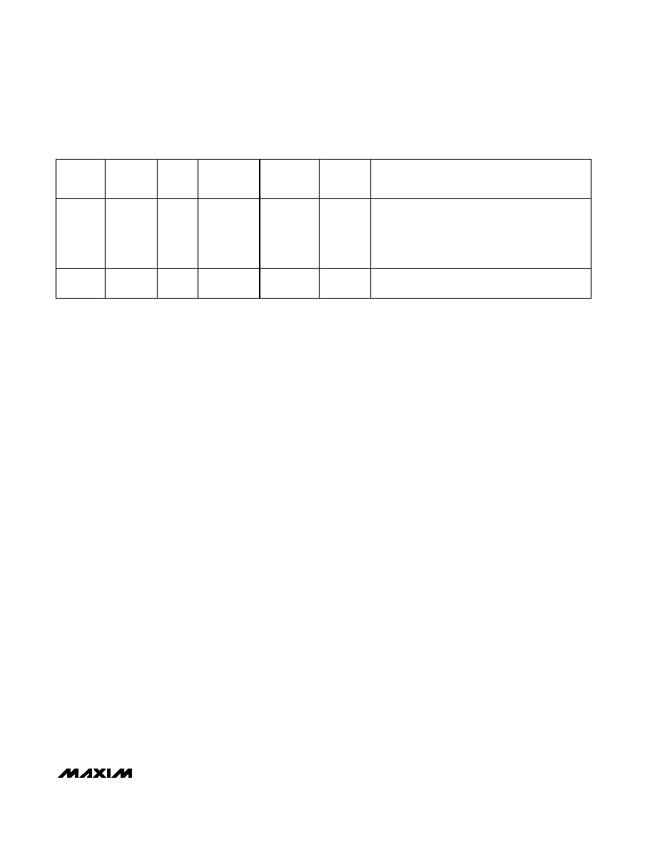
PART
I2C
SLAVE
ADDRESS
INPUTS
INPUT
INTERRUPT
MASK
OPEN-
DRAIN
OUTPUTS
PUSH-
PULL
OUTPUTS
CONFIGURATION
MAX7323
110xxxx
Up to 4
—
Up to 4
4
4 I/O, 4 output-only versions:
4 open-drain I/O ports with latching transition
detection interrupt and selectable pullups.
4 push-pull outputs with selectable power-up default
levels.
MAX7328
MAX7329
0100xxx
0111xxx
Up to 8
—
Up to 8
—
8 open-drain I/O ports with nonlatching transition
detection interrupt and pullups on all ports.
Table 1. MAX7319–MAX7329 Family Comparison (continued)
相关PDF资料 |
PDF描述 |
|---|---|
| MAX7323AEE+ | IC I/O EXPANDER I2C 4B 16QSOP |
| MAX7320ATE+ | IC I/O EXPANDER I2C 8B 16TQFN-EP |
| DS4520E+ | IC I/O EXPANDER I2C 9B 16TSSOP |
| MAX7315AEE+ | IC I/O EXPANDER I2C 8B 16QSOP |
| MAX7315AUE+ | IC I/O EXPANDER I2C 8B 16TSSOP |
相关代理商/技术参数 |
参数描述 |
|---|---|
| MAX7326ATG+ | 功能描述:接口-I/O扩展器 I2C Port Expander w/12 P-P Out & 4 In RoHS:否 制造商:NXP Semiconductors 逻辑系列: 输入/输出端数量: 最大工作频率:100 kHz 工作电源电压:1.65 V to 5.5 V 工作温度范围:- 40 C to + 85 C 安装风格:SMD/SMT 封装 / 箱体:HVQFN-16 封装:Reel |
| MAX7326ATG+T | 功能描述:接口-I/O扩展器 I2C Port Expander w/12 P-P Out & 4 In RoHS:否 制造商:NXP Semiconductors 逻辑系列: 输入/输出端数量: 最大工作频率:100 kHz 工作电源电压:1.65 V to 5.5 V 工作温度范围:- 40 C to + 85 C 安装风格:SMD/SMT 封装 / 箱体:HVQFN-16 封装:Reel |
| MAX7326ATG-T | 功能描述:接口-I/O扩展器 RoHS:否 制造商:NXP Semiconductors 逻辑系列: 输入/输出端数量: 最大工作频率:100 kHz 工作电源电压:1.65 V to 5.5 V 工作温度范围:- 40 C to + 85 C 安装风格:SMD/SMT 封装 / 箱体:HVQFN-16 封装:Reel |
| MAX7326EVCMAXQU+ | 功能描述:界面开发工具 MAX7326 Max7526 Kit RoHS:否 制造商:Bourns 产品:Evaluation Boards 类型:RS-485 工具用于评估:ADM3485E 接口类型:RS-485 工作电源电压:3.3 V |
| MAX7326EVKIT+ | 功能描述:界面开发工具 MAX7326 Eval Kit RoHS:否 制造商:Bourns 产品:Evaluation Boards 类型:RS-485 工具用于评估:ADM3485E 接口类型:RS-485 工作电源电压:3.3 V |
发布紧急采购,3分钟左右您将得到回复。