- 您现在的位置:买卖IC网 > PDF目录11015 > MAX7430EUB+T (Maxim Integrated Products)IC FILTER VIDEO SD 10-UMAX PDF资料下载
参数资料
| 型号: | MAX7430EUB+T |
| 厂商: | Maxim Integrated Products |
| 文件页数: | 4/21页 |
| 文件大小: | 0K |
| 描述: | IC FILTER VIDEO SD 10-UMAX |
| 产品培训模块: | Lead (SnPb) Finish for COTS Obsolescence Mitigation Program |
| 标准包装: | 2,500 |
| 滤波器类型: | 低通 |
| 频率 - 截止或中心: | 5MHz |
| 滤波器数: | 2 |
| 滤波器阶数: | 6th |
| 电源电压: | 4.5 V ~ 5.5 V |
| 安装类型: | 表面贴装 |
| 封装/外壳: | 10-TFSOP,10-MSOP(0.118",3.00mm 宽)裸露焊盘 |
| 供应商设备封装: | 10-µMAX-EP |
| 包装: | 带卷 (TR) |
MAX7428/MAX7430/MAX7432A
Standard Definition Video Reconstruction
Filters and Buffers
12
______________________________________________________________________________________
Programming the
MAX7428/MAX7430/MAX7432A
An address sequence precedes a write or read opera-
tion to determine with which device to communicate. If
the address transmitted in this mode matches with a
device’s address, the device and P can initiate data
transfer. When entering the four address bits, ensure
that the LSB is entered first. The following is the com-
mand sequence and timing diagram (Figure 6) for an
address sequence.
Use a write sequence to load data into the data register
of the device. It must follow an address sequence.
Transmit a minimum of eight data bits for the MAX7428,
16 data bits for the MAX7430, or 24 data bits for the
MAX7432A to make this transaction valid starting with
the LSB first. The last 8/16/24 data bits are used if more
than 8/16/24 bits are loaded into the register. The fol-
lowing is the command sequence and timing diagram
(Figure 7) for a write sequence.
During the read sequence, the P sends a prompt
pulse causing the device to output the data word LSB
first. Similar to the write transaction, the read transac-
tion must be preceded by an address sequence. If
more than 8 prompts (MAX7428), 16 prompts
(MAX7430), or 24 prompts (MAX7432A) are available,
the device outputs the same data starting with the LSB
again. The following is the command sequence and
timing diagram (Figure 8) for a read sequence.
Write Command Sequence:
T001
Data
≥ 8-bits (MAX7428,
See Table 1)
Data
≥ 16-bits (MAX7430,
See Table 3)
Data
≥ 24-bits (MAX7432A,
See Table 5)
T111
Address Command Sequence:
T010
Address = 4-bits
T111
Initialization Command Sequence:
Initialize wait
T011
Initialize Time Address ID = 4-bits
T111
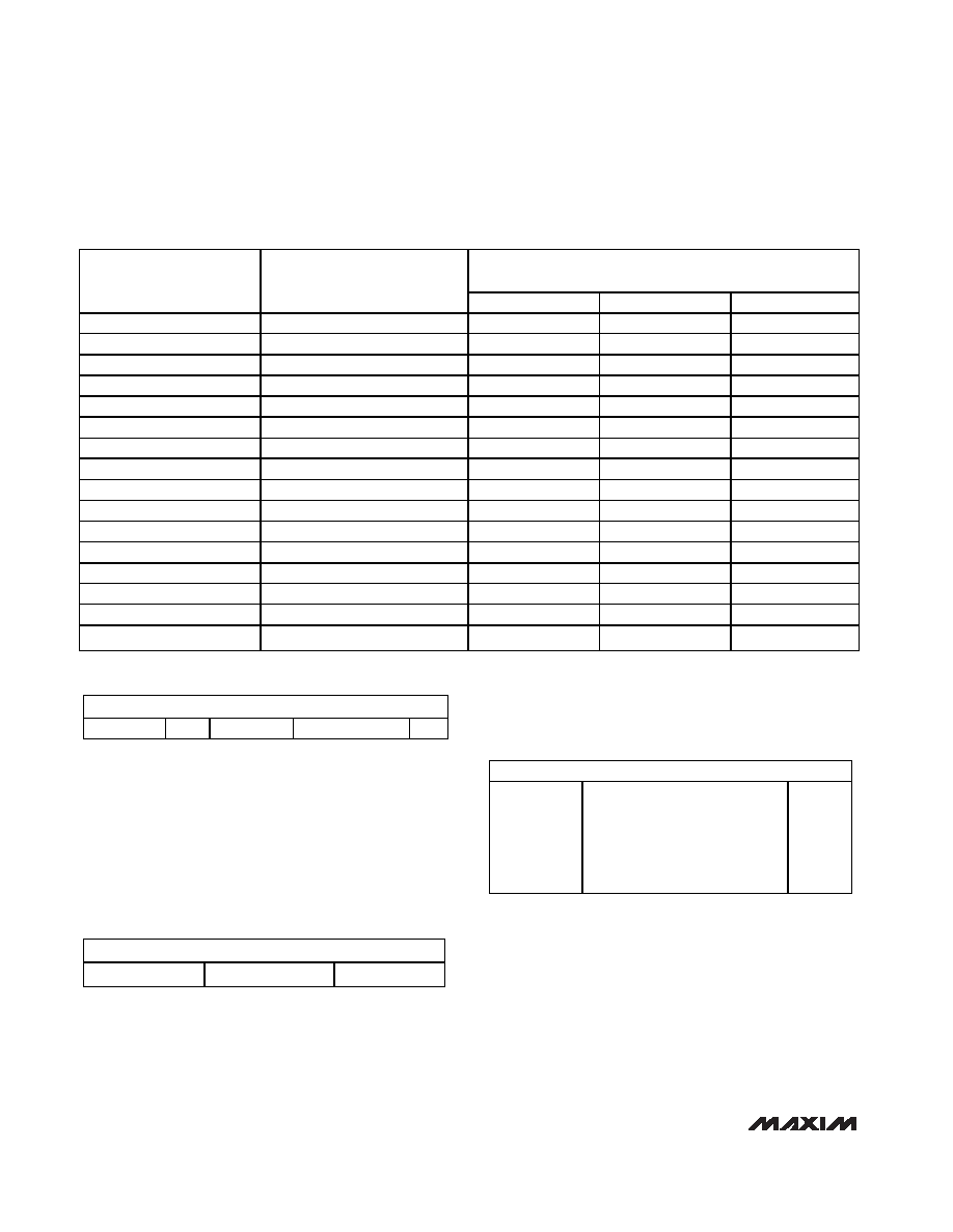
INITIALIZING TIME PERIOD (ms)
WITH RREXT = 300k
Ω (tINT)
CAPACITOR VALUE (nF)
INITIALIZING WAIT PERIOD
(ms) (tINTWAIT)
MIN
TYP
MAX
1000
20.000
162 (136.8)
171 (144)
179 (151.2)
680
13.600
112
118
123
470
9.400
52.6 (44.1)
55.4 (46.4)
58.2 (48.72)
220
4.400
35.90
37.80
39.70
150
3.000
23.90 (13.7)
25.20 (14.4)
26.50 (15.1)
100
2.000
16.25
17.10
17.95
68
1.360
11.21 (4.4)
11.80 (4.64)
12.39 (4.9)
47
0.940
5.26
5.54
5.82
22
0.440
3.59
3.78
3.97
15
0.300
2.39
2.52
2.65
10
0.200
1.625 (1.37)
1.710 (1.44)
1.795 (1.51)
6.8
0.136
1.121
1.180
1.239
4.7
0.094
0.526 (0.441)
0.554 (0.464)
0.582 (0.487)
2.2
0.044
0.359
0.378
0.397
1.5
0.030
0.239
0.252
0.265
1
0.020
0.162 (0.137)
0.171 (0.144)
0.179 (0.151)
Table 7. Initialization Capacitor Values and Pulse Widths
(CREXT = ±10% Tolerance, RREXT = ±1% Tolerance)
Note: ( ) Indicates the time periods associated with 20% capacitors. This limits the maximum number of devices on the bus to seven.
相关PDF资料 |
PDF描述 |
|---|---|
| MAX7444ETA+T | IC FILTER RECON VID 8-TDFN |
| VI-J1M-IW-B1 | CONVERTER MOD DC/DC 10V 100W |
| VE-J30-IW-B1 | CONVERTER MOD DC/DC 5V 100W |
| MAX7423CUA+ | IC FILTER LOWPASS 5TH 8UMAX |
| VI-JWN-IW-B1 | CONVERTER MOD DC/DC 18.5V 100W |
相关代理商/技术参数 |
参数描述 |
|---|---|
| MAX7432AEUD | 制造商:Rochester Electronics LLC 功能描述: 制造商:Maxim Integrated Products 功能描述: |
| MAX7432AEUD+ | 制造商:Rochester Electronics LLC 功能描述: 制造商:Maxim Integrated Products 功能描述: |
| MAX7432EUD | 功能描述:有源滤波器 RoHS:否 制造商:Maxim Integrated 通道数量:1 截止频率:150 KHz 电源电压-最大:11 V 电源电压-最小:4.74 V 最大工作温度:+ 85 C 安装风格:Through Hole 封装 / 箱体:PDIP N 封装:Tube |
| MAX7432EUD/GG8 | 功能描述:有源滤波器 RoHS:否 制造商:Maxim Integrated 通道数量:1 截止频率:150 KHz 电源电压-最大:11 V 电源电压-最小:4.74 V 最大工作温度:+ 85 C 安装风格:Through Hole 封装 / 箱体:PDIP N 封装:Tube |
| MAX7432EUD+ | 功能描述:视频 IC Standard Def Video Reconstruction Filtr RoHS:否 制造商:Fairchild Semiconductor 工作电源电压:5 V 电源电流:80 mA 最大工作温度:+ 85 C 封装 / 箱体:TSSOP-28 封装:Reel |
发布紧急采购,3分钟左右您将得到回复。