- 您现在的位置:买卖IC网 > PDF目录2089 > MAX7453CSA+ (Maxim Integrated Products)IC FILTER BUFFER VID 8-SOIC PDF资料下载
参数资料
| 型号: | MAX7453CSA+ |
| 厂商: | Maxim Integrated Products |
| 文件页数: | 2/5页 |
| 文件大小: | 0K |
| 描述: | IC FILTER BUFFER VID 8-SOIC |
| 产品培训模块: | Lead (SnPb) Finish for COTS Obsolescence Mitigation Program |
| 标准包装: | 100 |
| 类型: | 视频滤波器 |
| 应用: | DVD,游戏控制台,媒体播放器 |
| 安装类型: | 表面贴装 |
| 封装/外壳: | 8-SOIC(0.154",3.90mm 宽) |
| 供应商设备封装: | 8-SOIC |
| 包装: | 管件 |
MAX7453
Triple-Channel Video Reconstruction Filter and
Buffer for Composite and Y/C Outputs
2
_______________________________________________________________________________________
ABSOLUTE MAXIMUM RATINGS
Stresses beyond those listed under “Absolute Maximum Ratings” may cause permanent damage to the device. These are stress ratings only, and functional
operation of the device at these or any other conditions beyond those indicated in the operational sections of the specifications is not implied. Exposure to
absolute maximum rating conditions for extended periods may affect device reliability.
VCC to GND ...........................................................................+6V
All Other Pins to GND.................................-0.3V to (VCC + 0.3V)
Maximum Current into Any Pin Except VCC and GND .....±50mA
Continuous Power Dissipation (TA = +70°C)
8-Pin SO ....................................................................522.8mW
Operating Temperature Range...............................0°C to +70°C
Storage Temperature Range .............................-65°C to +150°C
Junction Temperature ......................................................+150°C
Lead Temperature (soldering, 10s) .................................+300°C
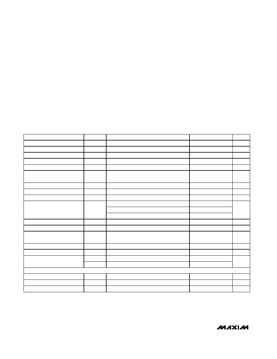
ELECTRICAL CHARACTERISTICS
(VCC = +5V ±5%, CL = 0 to 20pF, all loads to GND for DC-couple, all loads to VCC / 2 for AC-couple, CYIN = CCIN = 0.1F,
RYOUT = 150
Ω, RCOUT = 150Ω, RCVOUT = 75Ω, TA = TMIN to TMAX, unless otherwise noted. Typical values are at TA = +25°C.)
PARAMETER
SYMBOL
CONDITIONS
MIN
TYP
MAX
UNITS
Passband Response
f = 100kHz to 4.2MHz, relative to 100kHz
-0.6
-0.27
0
dB
Stopband Attenuation
ASB
f = 27MHz
39
42
dB
Chroma/Luma Gain
f = 3.58MHz, reference to CVOUT at 336kHz
96
98
100
%
Differential Gain
dG
5-step modulated staircase
0.15
0.5
%
Differential Phase
d
θ
5-step modulated staircase
0.15
0.5
Degrees
Signal-to-Noise Ratio
SNR
Peak signal (2VP-P) to RMS noise,
f = 100Hz to 50MHz
67
73
dB
Line-Time Distortion
HDIST
18s, 100IRE bar
0.3
%
Field-Time Distortion
VDIST
130 lines, 18s, 100IRE bar
0.5
%
Clamp Settling Time
To ±1%
300
Lines
YOUT
0.60
0.8
0.95
CVOUT
0.60
0.8
0.95
Output DC Clamp Level
COUT
1.44
1.6
1.95
V
Low-Frequency Gain Accuracy
AV
f = 100kHz, relative to 6dB
-3.0
+2.0
%
Group-Delay Deviation
Δtg
Deviation from 100kHz to 4.1MHz
8
16
ns
Group-Delay Matching
tg(MATCH)
Low-frequency channel-to-channel matching,
f = 100kHz for YOUT and COUT
2ns
Channel-to-Channel Crosstalk
XTALK
f = 100kHz to 3.58MHz
61
dB
Input Leakage Current
IIN
10
A
YINP-P
1.2
Input Dynamic Swing
CINP-P
0.9
VP-P
SUPPLY
Supply Voltage Range
VCC
4.75
5.25
V
Supply Current
ICC
VCC = +5.25V, no load
65
85
mA
Power-Supply Rejection Ratio
PSRR
VIN = 100mVP-P, f = 0 to 3.5MHz
33
dB
相关PDF资料 |
PDF描述 |
|---|---|
| MAX7456EUI+T | IC DISPLAY 1CH W/EEPROM 28TSSOP |
| MAX7461EUK+T | IC ALARM LOSS-OF-SYNC SOT23-5 |
| MAX7462USA+ | IC FILTER BUFFER VID 8-SOIC |
| MAX7474EAE+T | IC ADAPTV EQ VID OVER UTP 16SSOP |
| MAX8738EUA+T | IC CALIBR TFT VCOM 8UMAX |
相关代理商/技术参数 |
参数描述 |
|---|---|
| MAX7453CSA+ | 功能描述:视频 IC 3Ch Video Reconstruction Filtr RoHS:否 制造商:Fairchild Semiconductor 工作电源电压:5 V 电源电流:80 mA 最大工作温度:+ 85 C 封装 / 箱体:TSSOP-28 封装:Reel |
| MAX7453CSA+T | 功能描述:视频 IC 3Ch Video Reconstruction Filtr RoHS:否 制造商:Fairchild Semiconductor 工作电源电压:5 V 电源电流:80 mA 最大工作温度:+ 85 C 封装 / 箱体:TSSOP-28 封装:Reel |
| MAX7453CSA-T | 功能描述:有源滤波器 RoHS:否 制造商:Maxim Integrated 通道数量:1 截止频率:150 KHz 电源电压-最大:11 V 电源电压-最小:4.74 V 最大工作温度:+ 85 C 安装风格:Through Hole 封装 / 箱体:PDIP N 封装:Tube |
| MAX7453EVKIT+ | 功能描述:视频 IC 开发工具 MAX7453 Eval Kit RoHS:否 制造商:Texas Instruments 产品:Evaluation Boards 类型:YPbPr to RGBHV Converters 工具用于评估:LMH1251 工作电源电压:5 V |
| MAX7454EVKIT | 功能描述:视频 IC 开发工具 RoHS:否 制造商:Texas Instruments 产品:Evaluation Boards 类型:YPbPr to RGBHV Converters 工具用于评估:LMH1251 工作电源电压:5 V |
发布紧急采购,3分钟左右您将得到回复。