- 您现在的位置:买卖IC网 > PDF目录2012 > MAX7480ESA+T (Maxim Integrated Products)IC FILTER LOWPASS 8TH 8-SOIC PDF资料下载
参数资料
| 型号: | MAX7480ESA+T |
| 厂商: | Maxim Integrated Products |
| 文件页数: | 2/8页 |
| 文件大小: | 0K |
| 描述: | IC FILTER LOWPASS 8TH 8-SOIC |
| 产品培训模块: | Lead (SnPb) Finish for COTS Obsolescence Mitigation Program |
| 标准包装: | 2,500 |
| 滤波器类型: | 巴特沃斯,低通开关电容器 |
| 频率 - 截止或中心: | 2kHz |
| 滤波器数: | 4 |
| 滤波器阶数: | 8th |
| 电源电压: | 4.5 V ~ 5.5 V |
| 安装类型: | 表面贴装 |
| 封装/外壳: | 8-SOIC(0.154",3.90mm 宽) |
| 供应商设备封装: | 8-SOIC |
| 包装: | 带卷 (TR) |
MAX7480
8th-Order, Lowpass, Butterworth,
Switched-Capacitor Filter
2
_______________________________________________________________________________________
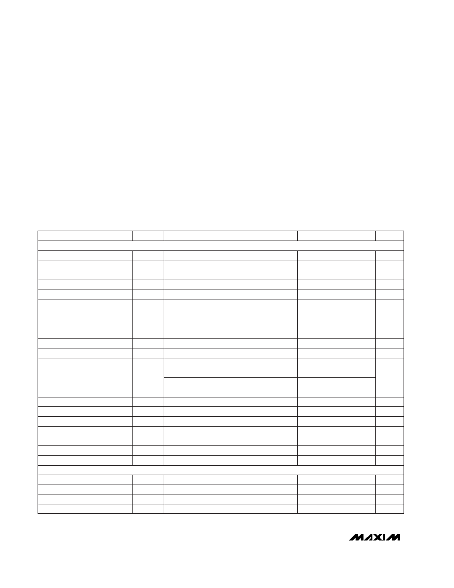
ABSOLUTE MAXIMUM RATINGS
ELECTRICAL CHARACTERISTICS
(VDD = +5V, filter output measured at OUT, 10k || 50pF load to GND at OUT, OS = COM, 0.1F from COM to GND, SHDN =
VDD, fCLK = 100kHz, TA = TMIN to TMAX, unless otherwise noted. Typical values are at TA = +25°C.)
Stresses beyond those listed under “Absolute Maximum Ratings” may cause permanent damage to the device. These are stress ratings only, and functional
operation of the device at these or any other conditions beyond those indicated in the operational sections of the specifications is not implied. Exposure to
absolute maximum rating conditions for extended periods may affect device reliability.
VDD to GND ..............................................................-0.3V to +6V
IN, OUT, COM, OS, CLK ............................-0.3V to (VDD + 0.3V)
SHDN........................................................................-0.3V to +6V
OUT Short-Circuit Duration...................................................1sec
Continuous Power Dissipation (TA = +70°C)
8-Pin SO (derate 5.88mW/°C above +70°C)................471mW
8-Pin DIP (derate 9.09mW/°C above +70°C) ...............727mW
Operating Temperature Range ...........................-40°C to +85°C
Storage Temperature Range .............................-65°C to +150°C
Lead Temperature (soldering, 10sec) .............................+300°C
COSC = 1000pF (Note 4)
VOS = 0 to (VDD - 1V) (Note 3)
SHDN = GND, VCOM = 0 to VDD
(Note 1)
Input, COM externally driven
fIN = 200Hz, VIN = 4Vp-p,
measurement bandwidth = 22kHz
VIN = VCOM = VDD / 2
VCOM = VDD / 2 (Note 2)
CONDITIONS
40
53
67
fOSC
Internal Oscillator Frequency
±0.1
±10
Input Leakage Current at OS
±0.1
±10
Input Leakage Current at COM
50
500
CL
10
1
RL
Resistive Output Load Drive
10
Clock Feedthrough
75
125
RCOM
Input Resistance at COM
100:1
fCLK /fC
Clock-to-Corner Ratio
0.001 to 2
fC
Corner Frequency
VCOM
1
AOS
OS Voltage Gain to OUT
-73
THD+N
Total Harmonic Distortion
plus Noise
10
Clock-to-Corner Tempco
0.25
VDD - 0.25
Output Voltage Range
±5
±25
VOFFSET
Output Offset Voltage
-0.1
0.15
0.3
DC Insertion Gain with
Output Offset Removed
MIN
TYP
MAX
SYMBOL
PARAMETER
VCLK = 0 or 5V
0.5
VIL
Clock Input Low
VDD - 0.5
VIH
Clock Input High
±24
±40
ICLK
Clock Input Current
V
A
kHz
A
pF
k
mVp-p
k
V
V/ V
dB
mV
V
ppm/°C
kHz
UNITS
Maximum Capacitive Load at
OUT
COM Voltage Range
VDD / 2
VDD / 2 VDD / 2
- 0.5
+ 0.5
VCOM ±0.1
VOS
Input Voltage Range at OS
V
VDD / 2
VDD / 2 VDD / 2
- 0.2
+ 0.2
FILTER CHARACTERISTICS
CLOCK
Output, COM internally biased
相关PDF资料 |
PDF描述 |
|---|---|
| MAX7491EEE+T | IC FILTER SW CAP DUAL 16-QSOP |
| MAX9501EEE+ | IC FILTER HDTV 16-QSOP |
| MAX9526AEI/V+T | IC VID DECODER NTSC/PAL 28QSOP |
| MAX98088EWY+T | IC CODEC AUDIO FLEXSOUND 63WLP |
| MAX98089ETN+ | IC CODEC AUDIO FLEXSOUND 56TQFN |
相关代理商/技术参数 |
参数描述 |
|---|---|
| MAX7481ETI+ | 制造商:Maxim Integrated Products 功能描述:HIGH-SPEED, LOW-VOLTAGE, 0.7O CMOS ANALOG SWITCHES/MULTIPLEX - Rail/Tube 制造商:Rochester Electronics LLC 功能描述: |
| MAX7482ETI+ | 制造商:Rochester Electronics LLC 功能描述: 制造商:Maxim Integrated Products 功能描述: |
| MAX748AC/D | 功能描述:直流/直流开关转换器 1.7mA Quiescent Current-Mode PWM DC-DC Converter RoHS:否 制造商:STMicroelectronics 最大输入电压:4.5 V 开关频率:1.5 MHz 输出电压:4.6 V 输出电流:250 mA 输出端数量:2 最大工作温度:+ 85 C 安装风格:SMD/SMT |
| MAX748AC/D DIE | 制造商:Maxim Integrated Products 功能描述: |
| MAX748ACPA | 功能描述:直流/直流开关转换器 3.3V Step-Down DC/DC Converter RoHS:否 制造商:STMicroelectronics 最大输入电压:4.5 V 开关频率:1.5 MHz 输出电压:4.6 V 输出电流:250 mA 输出端数量:2 最大工作温度:+ 85 C 安装风格:SMD/SMT |
发布紧急采购,3分钟左右您将得到回复。