- 您现在的位置:买卖IC网 > PDF目录2012 > MAX7491EEE+T (Maxim Integrated Products)IC FILTER SW CAP DUAL 16-QSOP PDF资料下载
参数资料
| 型号: | MAX7491EEE+T |
| 厂商: | Maxim Integrated Products |
| 文件页数: | 11/18页 |
| 文件大小: | 0K |
| 描述: | IC FILTER SW CAP DUAL 16-QSOP |
| 产品培训模块: | Lead (SnPb) Finish for COTS Obsolescence Mitigation Program |
| 标准包装: | 2,500 |
| 滤波器类型: | 通用开关电容器 |
| 频率 - 截止或中心: | 40kHz |
| 滤波器数: | 2 |
| 滤波器阶数: | 2nd |
| 电源电压: | 2.7 V ~ 3.6 V |
| 安装类型: | 表面贴装 |
| 封装/外壳: | 16-SSOP(0.154",3.90mm 宽) |
| 供应商设备封装: | 16-QSOP |
| 包装: | 带卷 (TR) |
MAX7490/MAX7491
Dual Universal Switched-Capacitor Filters
2
_______________________________________________________________________________________
ABSOLUTE MAXIMUM RATINGS
ELECTRICAL CHARACTERISTICS—MAX7490
(VDD = VEXTCLK = +5V; fCLK = 625kHz; 10kΩ || 50pF load to VDD/2 at LP_, BP_, and N_/HP_; VSHDN = VDD; 0.1F from COM to
GND; 50% duty-cycle clock input; COM = VDD/2; TA = TMIN to TMAX. Typical values are at TA = +25°C, unless otherwise noted.)
(Note 1)
Stresses beyond those listed under “Absolute Maximum Ratings” may cause permanent damage to the device. These are stress ratings only, and functional
operation of the device at these or any other conditions beyond those indicated in the operational sections of the specifications is not implied. Exposure to
absolute maximum rating conditions for extended periods may affect device reliability.
VDD to GND ..............................................................-0.3V to +6V
EXTCLK, SHDN to GND ...........................................-0.3V to +6V
INV_, LP_, BP_, N_/HP_, S_, COM,
CLK to GND............................................-0.3V to (VDD + 0.3V)
Maximum Current into Any Pin ...........................................50mA
Continuous Power Dissipation (TA = +70°C)
16-Pin QSOP (derate 8.30mW/°C above +70°C).........667mW
Operating Temperature Range
MAX749_CEE .....................................................0°C to +70°C
MAX749_EEE ...................................................-40°C to +85°C
Die Temperature ..............................................................+150°C
Storage Temperature.........................................-65°C to +150°C
Lead Temperature (soldering, 10s) .................................+300°C
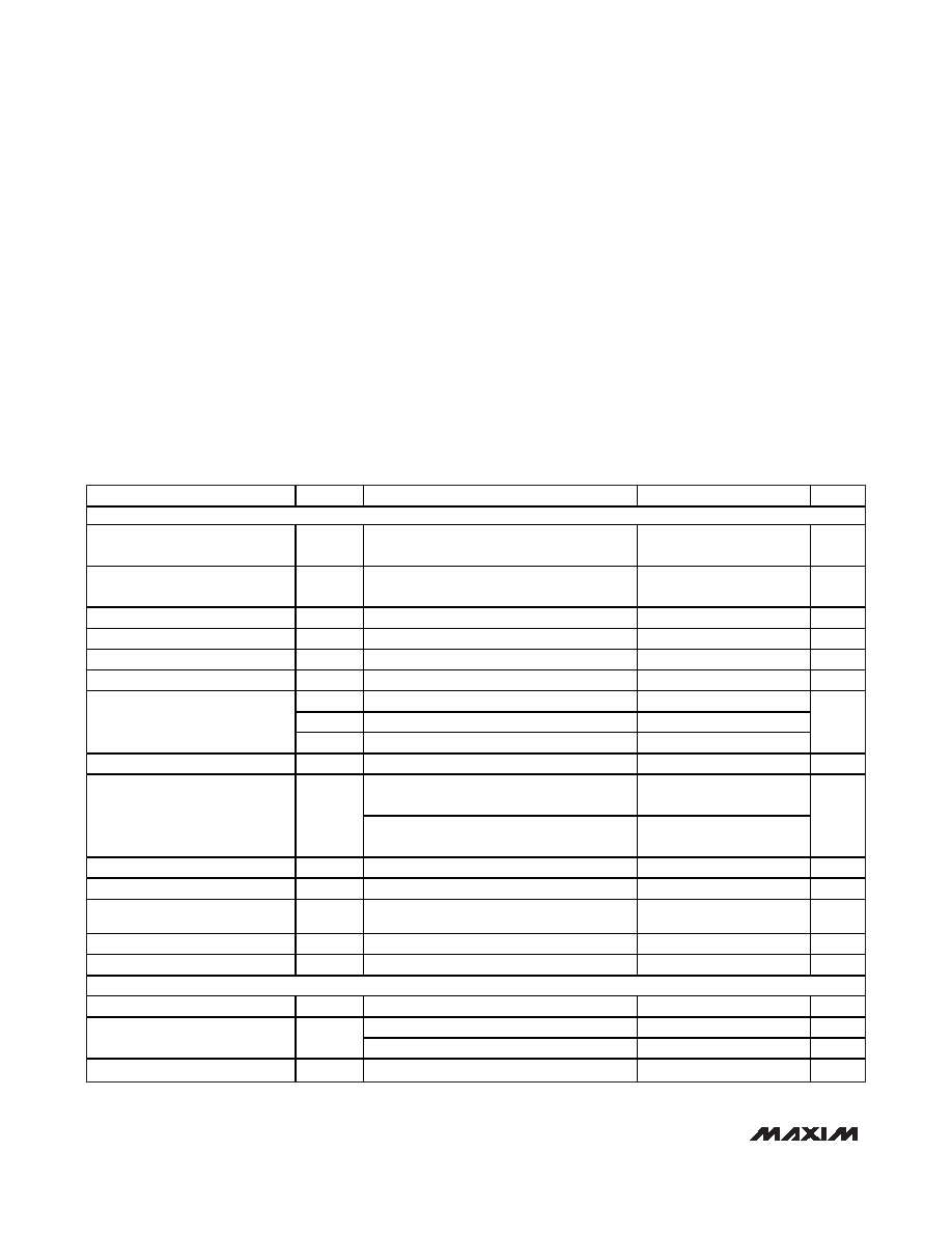
PARAMETER
SYMBOL
CONDITIONS
MIN
TYP
MAX
UNITS
FILTER
Center Frequency Range
fO
Mode 1
0.001 to
40
kHz
Clock-to-Center Frequency
Accuracy
fCLK/fO
Mode 1, R1 = R3 = 50k
Ω , R2 = 10kΩ,
Q = 5, deviation from 100:1
±0.2
±0.7
%
Q Accuracy
Mode 1, R1 = R3 = 50k
Ω, R2 = 10kΩ, Q = 5
±0.2
±2%
fO Temperature Coefficient
±1
ppm/
°C
Q Temperature Coefficient
±5
ppm/
°C
DC Lowpass Gain Accuracy
Mode 1, R1 = R2 = 10k
Ω±0.1
±0.5
%
VOS1
DC offset of input inverter
±3
±12.5
VOS2
DC offset of 1st integrator
±4
±15
DC Offset Voltage (Figure 8)
VOS3
DC offset of 2nd integrator
±4
±30
mV
Crosstalk (Note 2)
fIN = 10kHz
-60
dB
Input: COM externally driven
VDD/2
- 0.5
VDD/2
+ 0.5
COM Voltage Range
VCOM
Output: COM internally driven
VDD/2
- 0.2
VDD/2
+ 0.2
V
Input Resistance at COM
RCOM
140
250
325
k
Ω
Clock Feedthrough
Up to 5th harmonic of fCLK
200
μVRMS
Noise (Note 3)
Mode 1, R1 = R2 = R3 =10k
Ω, LP output,
Q = 1
60
μVRMS
Output Voltage Swing
0.2
VDD - 0.2
V
Input Leakage Current at COM
SHDN = GND, VCOM = 0 to VDD
±0.1
±10
μA
CLOCK
Maximum Clock Frequency
fCLK
4
MHz
EXTCLK = GND, COSC = 1000pF
95
135
175
kHz
Internal Oscillator Frequency
(Note 4)
fOSC
EXTCLK = GND, COSC = 100pF
1.35
MHz
Clock Input High
VDD - 0.5
V
相关PDF资料 |
PDF描述 |
|---|---|
| MAX9501EEE+ | IC FILTER HDTV 16-QSOP |
| MAX9526AEI/V+T | IC VID DECODER NTSC/PAL 28QSOP |
| MAX98088EWY+T | IC CODEC AUDIO FLEXSOUND 63WLP |
| MAX98089ETN+ | IC CODEC AUDIO FLEXSOUND 56TQFN |
| MAX9851ETM+T | IC CODEC AUDIO STEREO 48TQFN |
相关代理商/技术参数 |
参数描述 |
|---|---|
| MAX749C/D | 功能描述:显示驱动器和控制器 RoHS:否 制造商:Panasonic Electronic Components 工作电源电压:2.7 V to 5.5 V 最大工作温度: 安装风格:SMD/SMT 封装 / 箱体:QFN-44 封装:Reel |
| MAX749CPA | 功能描述:显示驱动器和控制器 Digitally Adjustable LCD Bias Supply RoHS:否 制造商:Panasonic Electronic Components 工作电源电压:2.7 V to 5.5 V 最大工作温度: 安装风格:SMD/SMT 封装 / 箱体:QFN-44 封装:Reel |
| MAX749CPA+ | 功能描述:显示驱动器和控制器 Digitally Adjustable LCD Bias Supply RoHS:否 制造商:Panasonic Electronic Components 工作电源电压:2.7 V to 5.5 V 最大工作温度: 安装风格:SMD/SMT 封装 / 箱体:QFN-44 封装:Reel |
| MAX749CPA+T | 制造商:Maxim Integrated Products 功能描述: |
| MAX749CSA | 功能描述:显示驱动器和控制器 Digitally Adjustable LCD Bias Supply RoHS:否 制造商:Panasonic Electronic Components 工作电源电压:2.7 V to 5.5 V 最大工作温度: 安装风格:SMD/SMT 封装 / 箱体:QFN-44 封装:Reel |
发布紧急采购,3分钟左右您将得到回复。