- 您现在的位置:买卖IC网 > PDF目录15138 > MAX774EPA+ (Maxim Integrated Products)IC REG CTRLR INV PWM 8-DIP PDF资料下载
参数资料
| 型号: | MAX774EPA+ |
| 厂商: | Maxim Integrated Products |
| 文件页数: | 11/16页 |
| 文件大小: | 0K |
| 描述: | IC REG CTRLR INV PWM 8-DIP |
| 产品培训模块: | Lead (SnPb) Finish for COTS Obsolescence Mitigation Program |
| 标准包装: | 50 |
| PWM 型: | 控制器 |
| 输出数: | 1 |
| 频率 - 最大: | 300kHz |
| 占空比: | 85% |
| 电源电压: | 3 V ~ 16.5 V |
| 降压: | 无 |
| 升压: | 无 |
| 回扫: | 无 |
| 反相: | 是 |
| 倍增器: | 无 |
| 除法器: | 无 |
| Cuk: | 无 |
| 隔离: | 无 |
| 工作温度: | -40°C ~ 85°C |
| 封装/外壳: | 8-DIP(0.300",7.62mm) |
| 包装: | 管件 |
�� �
�
�-5V/-12V/-15V� or� Adjustable,� High-Efficiency,�
�Low� I� Q� Inverting� DC-to-DC� Controllers�
�R� Z�
�0.1� μ� F�
�V� OUT�
�EXT� Drive� Voltages�
�EXT� swings� from� OUT� to� V+� and� provides� the� drive� out-�
�put� for� an� external� power� MOSFET.� When� using� the� on-�
�chip� feedback� resistors� for� the� preset� output� voltages,�
�the� voltage� at� OUT� equals� the� output� voltage.� When�
�R2�
�R1�
�1�
�2�
�OUT�
�FB�
�MAX774�
�MAX775�
�MAX776�
�GND�
�8�
�using� external� feedback� resistors,� OUT� may� be� tied� to�
�GND� or� some� other� potential� between� V� OUT� and� GND.�
�Always� observe� the� V+� to� OUT� absolute� maximum� rat-�
�ing� of� 21V.� For� V+� to� output� differentials� greater� than�
�21V,� OUT� must� be� tied� to� a� potential� more� positive� than�
�the� output� and,� therefore,� the� output� voltage� must� be�
�0.1� μ� F�
�4�
�REF�
�set� with� an� external� resistor� divider.�
�In� nonbootstrapped� operation� with� low� input� voltages�
�(<4V),� tie� OUT� to� a� negative� voltage� to� fully� enhance� the�
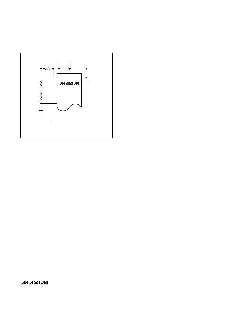
�___� =� _______�
�6V� ≤� V� Z� +� V� IN� ≤� 10V�
�?� VOUT� ?� –� V� Z�
�>� I� Z�
�R� Z�
�I� Z� =� ZENER� BREAKDOWN� CURRENT�
�V� Z� =� ZENER� BREAKDOWN� VOLTAGE�
�V� IN� =� INPUT� SUPPLY� VOLTAGE�
�Figure� 5.� Connection� Using� Zener� Diode� to� Boost� Base� Drive�
�connected� to� the� output� voltage� (-5V,� -12V,� -15V).� In�
�nonbootstrapped� operation,� OUT� is� connected� to�
�ground,� and� EXT� now� swings� from� V+� to� ground.�
�At� high� input-to-output� differentials,� it� may� be� neces-�
�sary� to� use� nonbootstrapped� mode� to� avoid� the� 21V� V+�
�to� V� OUT� maximum� rating.� Also,� observe� the� V� GS� maxi-�
�mum� rating� of� the� external� transistor.� At� intermediate�
�voltages� and� currents,� the� advantages� of� bootstrapped�
�vs.� nonbootstrapped� operation� are� slight.� When� input�
�voltages� are� less� than� about� 4V,� always� use� the� boot-�
�strapped� circuit.�
�Shutdown� and� Quiescent� Current�
�The� MAX774/MAX775/MAX776� are� designed� to� save�
�power� in� battery-powered� applications.� A� TTL/CMOS�
�logic-level� shutdown� input� (SHDN)� has� been� provided�
�for� the� lowest-power� applications.� When� shut� down�
�(SHDN� =� V+),� most� internal� bias� current� sources� and�
�the� reference� are� turned� off� so� that� less� than� 5μA� of�
�current� is� drawn.�
�In� normal� operation,� the� quiescent� current� will� be� less�
�than� 100μA.� However,� this� current� is� measured� by� forc-�
�ing� the� external� switch� transistor� off.� Even� with� no� load,�
�in� an� actual� application,� additional� current� will� be�
�drawn� to� supply� the� feedback� resistors’� and� the� diode’s�
�and� capacitor’s� leakage� current.� Under� no-load� condi-�
�tions,� you� should� see� a� short� current� pulse� at� half� the�
�peak� current� approximately� every� 100ms� (the� exact�
�period� depends� on� actual� circuit� leakages).�
�external� MOSFET.� Accomplish� this� by� creating� an� inter-�
�mediate� voltage� for� V� OUT� with� a� zener� diode� (Figure� 5).�
�__________________Design� Procedure�
�Setting� the� Output� Voltage�
�The� MAX774/MAX775/MAX776� are� preset� for� -5V,� -12V,�
�and� -15V� output� voltages,� respectively;� however,� they�
�may� also� be� adjusted� to� other� values� with� an� external�
�voltage� divider.� For� the� preset� output� voltage,� connect�
�FB� to� REF� and� connect� OUT� to� the� output� (Figure� 3).� In�
�this� case,� the� output� voltage� is� sensed� by� OUT.�
�For� an� adjustable� output� (Figures� 3� and� 4),� connect� an�
�external� resistor� divider� from� the� output� voltage� to� FB,�
�and� from� FB� to� REF.� In� this� case,� the� divided-down� out-�
�put� voltage� is� sensed� via� the� FB� pin.�
�There� are� three� reasons� to� use� the� external� resistor� divider:�
�1)� An� output� voltage� other� than� a� preset� value� is�
�desired.�
�2)� The� input-to-output� differential� exceeds� 21V.�
�3)� The� output� voltage� (V� OUT� to� GND)� exceeds� -15V.�
�See� Figures� 3� and� 4� for� adjustable� operation.� The�
�impedance� of� the� feedback� network� should� be� low�
�enough� that� the� input� bias� current� of� FB� is� not� a� factor.�
�For� best� efficiency� and� precision,� allow� 10μA� to� flow�
�through� the� network.� Calculate� (V� REF� -� V� FB� )� /� R1� =�
�10μA.� Since� V� REF� =� 1.5V� and� V� FB� =� 0V,� R1� becomes�
�150k� ?� .� Then� calculate� R2� as� follows:�
�R2� V� OUT�
�R1� V� REF�
�V� OUT�
�(or,� ______� =� 10� μ� A)�
�R2�
�Choosing� an� Inductor�
�Practical� inductor� values� range� from� 10μH� to� 50μH.�
�The� maximum� inductor� value� is� not� particularly� critical.�
�For� highest� current� at� high� ?� V� OUT� ?� to� V+� ratios,� the�
�______________________________________________________________________________________�
�11�
�相关PDF资料 |
PDF描述 |
|---|---|
| EB82-S0A2540X | CONN EDGEBOARD DUAL 50POS 5A |
| GBC65DRTN | CONN EDGECARD 130PS DIP .100 SLD |
| VI-25Z-EY-F4 | CONVERTER MOD DC/DC 2V 20W |
| VI-25Z-EY-F2 | CONVERTER MOD DC/DC 2V 20W |
| VI-25Z-EY-F1 | CONVERTER MOD DC/DC 2V 20W |
相关代理商/技术参数 |
参数描述 |
|---|---|
| MAX774EPA+ | 功能描述:DC/DC 开关控制器 5/12/15/AdjV- Inv DC/DC Controller RoHS:否 制造商:Texas Instruments 输入电压:6 V to 100 V 开关频率: 输出电压:1.215 V to 80 V 输出电流:3.5 A 输出端数量:1 最大工作温度:+ 125 C 安装风格: 封装 / 箱体:CPAK |
| MAX774ESA | 功能描述:DC/DC 开关控制器 5/12/15/AdjV- Inv DC/DC Controller RoHS:否 制造商:Texas Instruments 输入电压:6 V to 100 V 开关频率: 输出电压:1.215 V to 80 V 输出电流:3.5 A 输出端数量:1 最大工作温度:+ 125 C 安装风格: 封装 / 箱体:CPAK |
| MAX774ESA+ | 功能描述:DC/DC 开关控制器 5/12/15/AdjV- Inv DC/DC Controller RoHS:否 制造商:Texas Instruments 输入电压:6 V to 100 V 开关频率: 输出电压:1.215 V to 80 V 输出电流:3.5 A 输出端数量:1 最大工作温度:+ 125 C 安装风格: 封装 / 箱体:CPAK |
| MAX774ESA+T | 功能描述:DC/DC 开关控制器 5/12/15/AdjV- Inv DC/DC Controller RoHS:否 制造商:Texas Instruments 输入电压:6 V to 100 V 开关频率: 输出电压:1.215 V to 80 V 输出电流:3.5 A 输出端数量:1 最大工作温度:+ 125 C 安装风格: 封装 / 箱体:CPAK |
| MAX774ESA-T | 功能描述:DC/DC 开关控制器 5/12/15/AdjV- Inv DC/DC Controller RoHS:否 制造商:Texas Instruments 输入电压:6 V to 100 V 开关频率: 输出电压:1.215 V to 80 V 输出电流:3.5 A 输出端数量:1 最大工作温度:+ 125 C 安装风格: 封装 / 箱体:CPAK |
发布紧急采购,3分钟左右您将得到回复。