- 您现在的位置:买卖IC网 > PDF目录382287 > MAX829 (ON SEMICONDUCTOR) Switched Capacitor Voltage Converter PDF资料下载
参数资料
| 型号: | MAX829 |
| 厂商: | ON SEMICONDUCTOR |
| 元件分类: | 基准电压源/电流源 |
| 英文描述: | Switched Capacitor Voltage Converter |
| 中文描述: | 开关电容电压反相器 |
| 文件页数: | 6/18页 |
| 文件大小: | 158K |
| 代理商: | MAX829 |
MAX828, MAX829
http://onsemi.com
6
MAX828: C
1
= C
2
= C
3
= 10
F
MAX829: C
1
= C
2
= C
3
= 3.3 F
6
4
2
3
1
OSC
V
out
C
1
C
2
+
R
L
+
+C
3
V
in
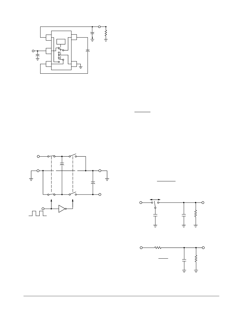
Figure 20. Test Setup/Voltage Inverter
DETAILED OPERATING DESCRIPTION
The MAX828/829 charge pump converters inverts the
voltage applied to the V
in
pin. Conversion consists of a
twophase operation (Figure 21). During the first phase,
switches S
2
and S
4
are open and S
1
and S
3
are closed. During
this time, C
1
charges to the voltage on V
in
and load current
is supplied from C
2
. During the second phase, S
2
and S
4
are
closed, and S
1
and S
3
are open. This action connects C
1
across C
2
, restoring charge to C
2
.
Figure 21. Ideal Switched Capacitor Charge Pump
S3
S4
C
2
C
1
S1
S2
V
in
V
out
From Osc
APPLICATIONS INFORMATION
Output Voltage Considerations
The MAX828/829 performs voltage conversion but does
not provide regulation. The output voltage will drop in a
linear manner with respect to load current. The value of this
equivalent output resistance is approximately 26 nominal
at 25
°
C and V
in
= 5.0 V. V
out
is approximately 5.0 V at light
loads, and drops according to the equation below:
VDROP
Iout
Rout
Vout
(Vin
VDROP)
Charge Pump Efficiency
The overall power efficiency of the charge pump is
affected by four factors:
1. Losses from power consumed by the internal
oscillator, switch drive, etc. (which vary with input
voltage, temperature and oscillator frequency).
2. I
2
R losses due to the onresistance of the MOSFET
switches onboard the charge pump.
3. Charge pump capacitor losses due to Equivalent
Series Resistance (ESR).
4. Losses that occur during charge transfer from the
commutation capacitor to the output capacitor when
a voltage difference between the two capacitors
exists.
Most of the conversion losses are due to factors 2, 3 and 4.
These losses are given by Equation 1.
PLOSS(2,3,4)
Iout
2
Rout
Iout
2
1
(fOSC)C1
8RSWITCH
4ESRC1
ESRC2
(eq. 1)
The 1/(f
OSC
)(C
1
) term in Equation 1 is the effective output
resistance of an ideal switched capacitor circuit (Figures 22
and 23).
The losses due to charge transfer above are also shown in
Equation 2. The output voltage ripple is given by Equation 3.
0.5C2(VRIPPLE
2
2VoutVRIPPLE)]
fOSC
PLOSS
[ 0.5C1(Vin
2
Vout
2
)
(eq. 2)
VRIPPLE
Iout
(fOSC)(C2)
2(Iout)(ESRC2)
(eq. 3)
R
L
C
2
C
1
V
in
V
out
f
Figure 22. Ideal Switched Capacitor Model
R
L
C
2
V
in
V
out
R
EQUIV
REQUIV
1
f
C1
Figure 23. Equivalent Output Resistance
相关PDF资料 |
PDF描述 |
|---|---|
| MAX829EUK | Parallel-Load 8-Bit Shift Registers 16-CDIP -55 to 125 |
| MAX828EUKG | Switched Capacitor Voltage Converter |
| MAX829EUKG | Switched Capacitor Voltage Converter |
| MAX828SNTR | Switched Capacitor Voltage Converters |
| MAX829SNTR | Switched Capacitor Voltage Converters |
相关代理商/技术参数 |
参数描述 |
|---|---|
| MAX829C/D | 制造商:MAXIM 制造商全称:Maxim Integrated Products 功能描述:Switched-Capacitor Voltage Inverters |
| MAX829C/D DIE | 制造商:Maxim Integrated Products 功能描述: |
| MAX829EUK | 功能描述:电荷泵 Switched Cap Voltage RoHS:否 制造商:Maxim Integrated 功能:Inverting, Step Up 输出电压:- 1.5 V to - 5.5 V, 3 V to 11 V 输出电流:100 mA 电源电流:1 mA 最大工作温度:+ 70 C 封装 / 箱体:SOIC-8 Narrow 封装:Tube |
| MAX829EUK+ | 制造商:Maxim Integrated Products 功能描述:CHG PUMP INV -5.5V TO -1.5V 25MA 5PIN SOT-23 - Rail/Tube |
| MAX829EUK+T | 功能描述:电荷泵 Switched-Capacitor Voltage Inverter RoHS:否 制造商:Maxim Integrated 功能:Inverting, Step Up 输出电压:- 1.5 V to - 5.5 V, 3 V to 11 V 输出电流:100 mA 电源电流:1 mA 最大工作温度:+ 70 C 封装 / 箱体:SOIC-8 Narrow 封装:Tube |
发布紧急采购,3分钟左右您将得到回复。