- 您现在的位置:买卖IC网 > PDF目录19825 > MAX8517EUB+T (Maxim Integrated)IC REG LDO ADJ 1A 10-UMAX PDF资料下载
参数资料
| 型号: | MAX8517EUB+T |
| 厂商: | Maxim Integrated |
| 文件页数: | 7/10页 |
| 文件大小: | 0K |
| 描述: | IC REG LDO ADJ 1A 10-UMAX |
| 产品培训模块: | Lead (SnPb) Finish for COTS Obsolescence Mitigation Program |
| 标准包装: | 2,500 |
| 稳压器拓扑结构: | 正,可调式 |
| 输出电压: | 0.5 V ~ 3.4 V |
| 输入电压: | 1.43 V ~ 3.6 V |
| 电压 - 压降(标准): | 0.1V @ 1A |
| 稳压器数量: | 1 |
| 电流 - 输出: | 1A |
| 电流 - 限制(最小): | 1.6A |
| 工作温度: | -40°C ~ 85°C |
| 安装类型: | 表面贴装 |
| 封装/外壳: | 10-TFSOP,10-MSOP(0.118",3.00mm 宽)裸露焊盘 |
| 供应商设备封装: | 10-µMAX-EP |
| 包装: | 带卷 (TR) |
�� �
�
�1.425V� to� 3.6V� Input,� 1A,�
�0.2V� Dropout� LDO� Regulators�
�Detailed� Description�
�The� MAX8516/MAX8517/MAX8518� are� low-input,� low-�
�dropout,� PMOS� regulators� capable� of� delivering� up� to�
�1A� of� output� current� with� as� little� as� 200mV� of� headroom�
�from� input� to� output.� The� PMOS� output� stage� can� be� dri-�
�ven� from� input� voltages� down� to� +1.425V� without� sacri-�
�Output� Voltage� Selection�
�The� MAX8516/MAX8517/MAX8518� feature� an�
�adjustable� output� voltage� from� 0.5V� to� 3.4V,� using� two�
�external� resistors� connected� as� a� voltage-divider� to� FB�
�as� shown� in� Figure� 1.� The� output� voltage� is� set� by� the�
�following� equation:�
�V� OUT� FB� ?� 1� +�
�=� V�
�R� 2� ?�
�ficing stability or transient performance. Since these�
�regulators� have� a� PMOS� output� device,� supply� current�
�is� not� a� significant� function� of� load� or� input� headroom.�
�?�
�?�
�R� 1� ?�
�?�
�Internal� p-Channel� Pass� Transistor�
�The� MAX8516/MAX8517/MAX8518� feature� a� 100m� ?� (typ)�
�p-channel� MOSFET� pass� transistor.� Unlike� similar�
�designs� using� pnp� pass� transistors,� p-channel� MOSFETs�
�where� typically� V� FB� =� 0.5V.� Choose� R2� ≤� 5k� ?� to� opti-�
�mize� quiescent� current,� accuracy,� and� high-frequency�
�power-supply� rejection.� To� simplify� resistor� selection:�
�R� 1� =� R� 2� ?� OUT�
�1� ?�
�require no base drive, which reduces quiescent current.�
�pnp-based� regulators� also� waste� considerable� current� in�
�dropout� when� the� pass� transistor� saturates� and� use� high�
�?� V�
�?� V� FB�
�?�
�?�
�?�
�I� INRUSH� =� I� LOAD� +� ?� OUT�
�?�
�?�
�?�
�base-drive currents under large loads. The MAX8516/�
�MAX8517/MAX8518� do� not� suffer� from� these� problems�
�and� consume� only� 340μA� (typ)� of� quiescent� current�
�under� heavy� loads,� as� well� as� in� dropout.�
�Short-Circuit/Thermal� Fault� Protection�
�The� MAX8516/MAX8517/MAX8518� are� fully� protected�
�from� a� short� circuit� at� the� output� through� current-limiting�
�and� thermal-overload� circuitry.� In� the� fault� condition�
�when� the� output� is� shorted� to� ground,� the� output� current�
�is� limited� to� 2A.� Under� these� conditions,� the� part� quickly�
�heats� up.� When� the� junction� temperature� reaches�
�+165°C,� the� thermal-overload� circuitry� turns� off� the�
�output,� allowing� the� part� to� cool� down.� When� the� junction�
�temperature� cools� to� +150°C,� the� output� turns� back� on�
�and� tries� to� reestablish� regulation.� Current� limiting� and�
�thermal� protection� continue� until� the� fault� is� removed.� For�
�continuous� operation,� do� not� exceed� the� absolute� maxi-�
�mum� junction-temperature� rating� of� T� J� =� +150°C.�
�ADJUSTABLE�
�Soft-Start�
�Inherent� soft-start� limits� inrush� current.� Peak� inrush� cur-�
�rent� is� dependent� on� the� value� of� C� OUT� and� can� be� cal-�
�culated� as� follows:�
�?� C (� μ� F)� ?�
�66�
�Shutdown� Mode�
�The� MAX8516/MAX8517/MAX8518� include� an� enable�
�input.� To� shut� down� the� device,� pull� EN� to� GND.� For�
�normal� operation,� connect� the� EN� to� IN.� During� shut-�
�down,� an� internal� 10k� ?� resistor� pulls� down� the� output.�
�Power-OK� (MAX8517� Only)�
�The� MAX8517� features� a� power-OK� (POK)� output� to�
�indicate� the� status� of� the� output.� POK� remains� high�
�when� the� regulator� output� is� within� ±10%� of� its� nominal�
�output� voltage.� If� the� output� voltage� falls� or� rises� out-�
�side� this� range,� POK� transitions� low.� This� open-drain�
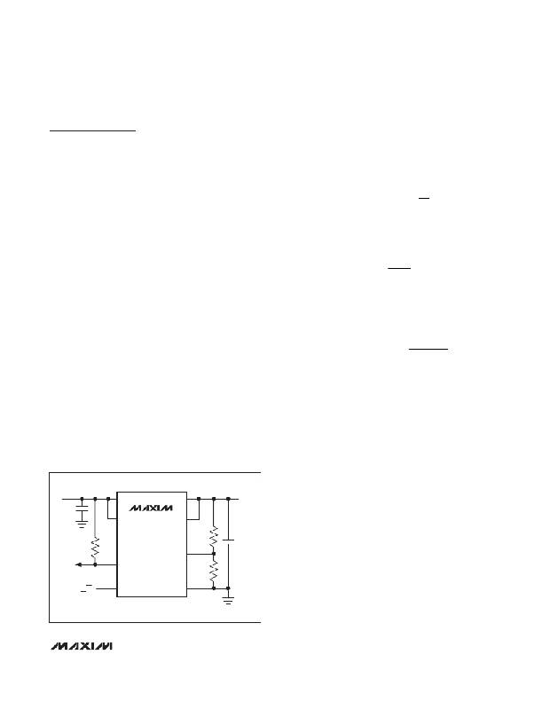
�+1.425V� TO� +3.6V�
�1� μ� F�
�IN�
�IN�
�MAX8516�
�MAX8517�
�OUT�
�OUT�
�OUTPUT�
�output� requires� an� external� pullup� resistor� to� IN.� An�
�internal� delay� circuit� prevents� POK� from� switching� for�
�50μs� (typ)� after� the� trip� threshold� is� initially� reached.� If�
�the� part� is� in� shutdown� mode,� POK� is� low.�
�100k� ?� *�
�ENABLE�
�MAX8518�
�POK� (MAX8517)� OR�
�POR� (MAX8518)�
�EN�
�FB�
�GND�
�R1�
�R2�
�4.7� μ� F�
�Power-On� Reset� (MAX8518� Only)�
�The� MAX8518� features� a� power-on� reset� (POR)� output�
�that� transitions� high� 140ms� (typ)� after� the� output� has�
�risen� above� 90%� of� its� final� value.� This� open-drain� out-�
�put� requires� an� external� pullup� resistor� to� IN.� If� the� part�
�is� in� shutdown� mode,� falls� below� 90%� of� the� nominal�
�SHUTDOWN�
�*FOR� MAX8517� AND� MAX8518�
�Figure� 1.� Typical� Application� Circuit�
�output� voltage,� or� experiences� a� short-circuit� or� thermal�
�fault,� POR� immediately� transitions� low.�
�_______________________________________________________________________________________�
�7�
�相关PDF资料 |
PDF描述 |
|---|---|
| TAP107M020CCS | CAP TANT 100UF 20V 20% RADIAL |
| VE-24Y-CW-B1 | CONVERTER MOD DC/DC 3.3V 66W |
| 4-641285-8 | 18 CIR MTA 156 EDG CON F/T LF |
| GMA50DRMD | CONN EDGECARD 100POS .125 SQ WW |
| CWR29MB106KBHZ | CAP TANT 10UF 35V 10% 2915 |
相关代理商/技术参数 |
参数描述 |
|---|---|
| MAX8517EVKIT+ | 功能描述:电源管理IC开发工具 MAX8517 Eval Kit RoHS:否 制造商:Maxim Integrated 产品:Evaluation Kits 类型:Battery Management 工具用于评估:MAX17710GB 输入电压: 输出电压:1.8 V |
| MAX8518EUB | 功能描述:低压差稳压器 - LDO RoHS:否 制造商:Texas Instruments 最大输入电压:36 V 输出电压:1.4 V to 20.5 V 回动电压(最大值):307 mV 输出电流:1 A 负载调节:0.3 % 输出端数量: 输出类型:Fixed 最大工作温度:+ 125 C 安装风格:SMD/SMT 封装 / 箱体:VQFN-20 |
| MAX8518EUB+ | 功能描述:低压差稳压器 - LDO 1.425V to 3.6V Input 1A 0.2V Dropout LDO RoHS:否 制造商:Texas Instruments 最大输入电压:36 V 输出电压:1.4 V to 20.5 V 回动电压(最大值):307 mV 输出电流:1 A 负载调节:0.3 % 输出端数量: 输出类型:Fixed 最大工作温度:+ 125 C 安装风格:SMD/SMT 封装 / 箱体:VQFN-20 |
| MAX8518EUB+T | 功能描述:低压差稳压器 - LDO 1.425V to 3.6V Input 1A 0.2V Dropout LDO RoHS:否 制造商:Texas Instruments 最大输入电压:36 V 输出电压:1.4 V to 20.5 V 回动电压(最大值):307 mV 输出电流:1 A 负载调节:0.3 % 输出端数量: 输出类型:Fixed 最大工作温度:+ 125 C 安装风格:SMD/SMT 封装 / 箱体:VQFN-20 |
| MAX8518EUB-T | 功能描述:低压差稳压器 - LDO RoHS:否 制造商:Texas Instruments 最大输入电压:36 V 输出电压:1.4 V to 20.5 V 回动电压(最大值):307 mV 输出电流:1 A 负载调节:0.3 % 输出端数量: 输出类型:Fixed 最大工作温度:+ 125 C 安装风格:SMD/SMT 封装 / 箱体:VQFN-20 |
发布紧急采购,3分钟左右您将得到回复。