- 您现在的位置:买卖IC网 > PDF目录16555 > MAX8520ETP+T (Maxim Integrated Products)IC DRVR PWR TEC 20-TQFN PDF资料下载
参数资料
| 型号: | MAX8520ETP+T |
| 厂商: | Maxim Integrated Products |
| 文件页数: | 2/18页 |
| 文件大小: | 0K |
| 描述: | IC DRVR PWR TEC 20-TQFN |
| 产品培训模块: | Lead (SnPb) Finish for COTS Obsolescence Mitigation Program |
| 标准包装: | 2,500 |
| 应用: | 热电冷却器 |
| 电源电压: | 3 V ~ 5.5 V |
| 工作温度: | -40°C ~ 85°C |
| 安装类型: | 表面贴装 |
| 封装/外壳: | 20-WQFN 裸露焊盘 |
| 供应商设备封装: | 20-TQFN-EP(5x5) |
| 包装: | 带卷 (TR) |
�� �
�
�Smallest� TEC� Power� Drivers� for� Optical�
�Modules�
�ABSOLUTE� MAXIMUM� RATINGS�
�V� DD� to� GND� ..............................................................-0.3V� to� +6V�
�SHDN� ,� MAXV,� MAXIP,� MAXIN,�
�CTLI� to� GND� .........................................................-0.3V� to� +6V�
�COMP,� FREQ,� OS1,� OS2,� CS,� REF,�
�ITEC� to� GND...........................................-0.3V� to� (V� DD� +� 0.3V)�
�PVDD1,� PVDD2� to� GND� .............................-0.3V� to� (V� DD� +� 0.3V)�
�PVDD1,� PVDD2� to� V� DD� ..........................................-0.3V� to� +0.3V�
�PGND1,� PGND2� to� GND� .......................................-0.3V� to� +0.3V�
�COMP,� REF,� ITEC� short� to� GND....................................Indefinite�
�LX� Current� (Note� 1)� ........................................±2.25A� LX� Current�
�Continuous� Power� Dissipation� (T� A� =� +70°C)�
�6� x� 6� UCSP� (derate� 22mW/°C� above� +70°C)� ...............1.75W�
�20-Pin� 5mm� x� 5mm� x� 0.9mm� TQFN� (derate� 20.8mW/°C�
�above� +70°C)� (Note� 2)...................................................1.67W�
�36-Bump� WLP� (derate� 22mW/°C� above� +70°C)............1.75W�
�Operating� Temperature� Range� ...........................-40°C� to� +85°C�
�Maximum� Junction� Temperature� .....................................+150°C�
�Storage� Temperature� Range� .............................-65°C� to� +150°C�
�Lead� Temperature� (soldering,� 10s)� .................................+300°C�
�Soldering� Temperature� (reflow)�
�Lead(Pb)-Free� (TQFN,� WLP)........................................+260°C�
�Containing� Lead� (UCSP).............................................� +240°C�
�Stresses� beyond� those� listed� under� “Absolute� Maximum� Ratings”� may� cause� permanent� damage� to� the� device.� These� are� stress� ratings� only,� and� functional�
�operation� of� the� device� at� these� or� any� other� conditions� beyond� those� indicated� in� the� operational� sections� of� the� specifications� is� not� implied.� Exposure� to�
�absolute� maximum� rating� conditions� for� extended� periods� may� affect� device� reliability.�
�Note� 1:� LX� has� internal� clamp� diodes� to� PGND� and� PVDD.� Applications� that� forward� bias� these� diodes� should� take� care� not� to�
�exceed� the� IC’s� package� power� dissipation� limits.�
�Note� 2:� Solders� underside� metal� slug� to� PCB� ground� plane.�
�PACKAGE� THERMAL� CHARACTERISTICS� (Note� 3)�
�20� TQFN�
�Junction-to-Ambient� Thermal� Resistance� (� θ� JA� )...............30°C/W�
�Junction-to-Case� Thermal� Resistance� (� θ� JC� )......................2°C/W�
�36� WLP�
�Junction-to-Ambient� Thermal� Resistance� (� θ� JA� )..................38°C/W�
�Junction-to-Case� Thermal� Resistance� (� θ� JC� )......................4°C/W�
�6x6� UCSP�
�Junction-to-Ambient� Thermal� Resistance� (� θ� JA� )................65.5°C/W�
�Junction-to-Case� Thermal� Resistance� (� θ� JC� ).......................0°C/W�
�Note� 3:� Package� thermal� resistances� were� obtained� using� the� method� described� in� JEDEC� specification� JESD51-7,� using� a� four-�
�layer� board.� For� detailed� information� on� package� thermal� considerations,� refer� to� www.maxim-ic.com/thermal-tutorial� .�
�ELECTRICAL� CHARACTERISTICS�
�(V� DD� =� V� PVDD1� =� V� PVDD2� =� V� SHDN� =� 5V,� 1MHz� mode� (Note� 4).� PGND1� =� PGND2� =� GND,� CTLI� =� MAXV� =� MAXIP� =� MAXIN� =� REF,�
�T� A� =� 0°C� to� +85°C� ,� unless� otherwise� noted.� Typical� values� at� T� A� =� +25°C.)�
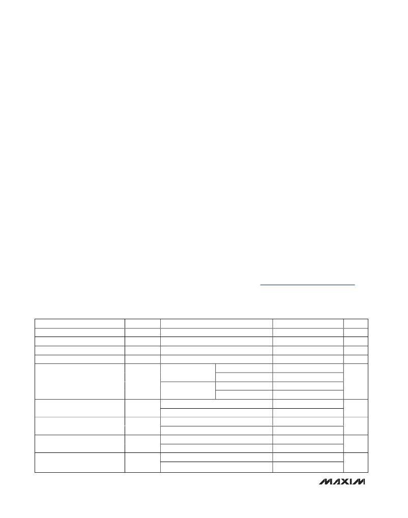
�PARAMETER�
�Input� Supply� Range�
�SYMBOL�
�V� DD�
�CONDITIONS�
�MIN�
�3.0�
�TYP�
�MAX�
�5.5�
�UNITS�
�V�
�Maximum� TEC� Current�
�±� 1.5�
�A�
�Reference� Voltage�
�Reference� Load� Regulation�
�V� REF�
�?� V� REF�
�V� DD� =� 3V� to� 5.5V,� I� REF� =� 150μA�
�V� DD� =� 3V� to� 5V,� I� REF� =� 10μA� to� 1mA�
�1.485�
�1.500�
�1.2�
�1.515�
�5.0�
�V�
�mV�
�MAXIP/MAXIN� Threshold�
�Accuracy�
�V� DD� =� 5V�
�V� DD� =� 3V�
�V� MAXI_� =� V� REF�
�V� MAXI_� =� V� REF� /3�
�V� MAXI_� =� V� REF�
�V� MAXI_� =� V� REF� /3�
�140�
�40�
�143�
�45�
�150�
�50�
�150�
�50�
�160�
�60�
�155�
�55�
�mV�
�nFET� On-Resistance�
�pFET� On-Resistance�
�nFET� Leakage�
�pFET� Leakage�
�R� DS(ON-N)�
�R� DS(ON-P)�
�I� LEAK(N)�
�I� LEAK(P)�
�V� DD� =� 5V,� I� =� 0.2A�
�V� DD� =� 3V,� I� =� 0.2A�
�V� DD� =� 5V,� I� =� 0.2A�
�V� DD� =� 3V,� I� =� 0.2A�
�V� LX� =� V� DD� =� 5V,� T� A� =� +25� °� C�
�V� LX� =� V� DD� =� 5V� T� A� =� +85� °� C�
�V� LX� =� 0V,� T� A� =� +25� °� C�
�V� LX� =� 0V,� T� A� =� +85� °� C�
�0.09�
�0.11�
�0.14�
�0.17�
�0.03�
�0.3�
�0.03�
�0.3�
�0.14�
�0.16�
�0.23�
�0.30�
�4.00�
�4.00�
�?�
�?�
�μA�
�μA�
�2�
�_______________________________________________________________________________________�
�相关PDF资料 |
PDF描述 |
|---|---|
| ECM24DRKH | CONN EDGECARD 48POS DIP .156 SLD |
| XR16M681IL24-0C-EB | EVAL BOARD FOR XR16M681-C 24QFN |
| EEM36DCAN | CONN EDGECARD 72POS R/A .156 SLD |
| H3CKH-2618G | IDC CABLE - HKC26H/AE26G/HPK26H |
| MAX8521ETP+T | IC DRVR PWR TEC 20-TQFN |
相关代理商/技术参数 |
参数描述 |
|---|---|
| MAX8520EVKIT | 制造商:Maxim Integrated Products 功能描述:SMALLEST TEC POWER DRIVERS FOR OPTI - Rail/Tube |
| MAX8521EBX | 制造商:Maxim Integrated Products 功能描述:SMALLEST TEC POWER DRIVERS FOR OPTICAL MODULE - Rail/Tube |
| MAX8521EBX+T | 功能描述:其他电源管理 RoHS:否 制造商:Texas Instruments 输出电压范围: 输出电流:4 mA 输入电压范围:3 V to 3.6 V 输入电流: 功率耗散: 工作温度范围:- 40 C to + 110 C 安装风格:SMD/SMT 封装 / 箱体:VQFN-48 封装:Reel |
| MAX8521EBX-T | 功能描述:其他电源管理 RoHS:否 制造商:Texas Instruments 输出电压范围: 输出电流:4 mA 输入电压范围:3 V to 3.6 V 输入电流: 功率耗散: 工作温度范围:- 40 C to + 110 C 安装风格:SMD/SMT 封装 / 箱体:VQFN-48 封装:Reel |
| MAX8521ETP | 功能描述:其他电源管理 RoHS:否 制造商:Texas Instruments 输出电压范围: 输出电流:4 mA 输入电压范围:3 V to 3.6 V 输入电流: 功率耗散: 工作温度范围:- 40 C to + 110 C 安装风格:SMD/SMT 封装 / 箱体:VQFN-48 封装:Reel |
发布紧急采购,3分钟左右您将得到回复。