- 您现在的位置:买卖IC网 > PDF目录1847 > MAX852ESA+T (Maxim Integrated Products)IC REG SWITCHED CAP INV 8SOIC PDF资料下载
参数资料
| 型号: | MAX852ESA+T |
| 厂商: | Maxim Integrated Products |
| 文件页数: | 7/8页 |
| 文件大小: | 0K |
| 描述: | IC REG SWITCHED CAP INV 8SOIC |
| 标准包装: | 2,500 |
| 类型: | 切换式电容器(充电泵),反相 |
| 输出类型: | 两者兼有 |
| 输出数: | 1 |
| 输出电压: | -4.1V,-0.5 V ~ -9 V |
| 输入电压: | 4.5 V ~ 10 V |
| 频率 - 开关: | 100kHz |
| 电流 - 输出: | 5mA |
| 同步整流器: | 无 |
| 工作温度: | -40°C ~ 85°C |
| 安装类型: | 表面贴装 |
| 封装/外壳: | 8-SOIC(0.154",3.90mm 宽) |
| 包装: | 带卷 (TR) |
| 供应商设备封装: | 8-SOIC |
�� �
�
�Low-Noise,� Regulated,� Negative�
�Charge-Pump� Power� Supplies� for� GaAsFET� Bias�
�__________Applications� Information�
�V� IN�
�Setting� the� Output� Voltage�
�For� the� MAX850–MAX852,� select� either� a� fixed� or� an�
�adjustable� output� voltage.� Connect� FB� directly� to� GND� to�
�select� the� fixed� -4.1V� output� (Figure� 2a).� To� select� an� alter-�
�C1�
�1� μ� F�
�C1+�
�IN�
�C3�
�1� μ� F�
�V� OUT� =� -0.5V� to� -9V� @� 5mA�
�(�
�)�
�V� OUT� =� -1.28� ?� 1� +�
�R� 1� ?�
�nate� output� voltage,� connect� FB� to� the� midpoint� of� a� resis-�
�tor� voltage� divider� from� OUT� to� GND� (Figure� 2b).� V� IN� must�
�be� 1.0V� above� the� absolute� value� of� V� OUT� to� allow� proper�
�regulation.� The� output� voltage� is� calculated� from� the� formu-�
�la� below.� Choose� R2� to� be� between� 100k� ?� to� 400k� ?� .�
�?�
�R� 2� ?�
�?�
�?�
�C2�
�1� μ� F�
�C1-� MAX853�
�NEGOUT�
�SHDN�
�GND�
�OUT�
�CONT�
�R2�
�100k�
�R1�
�100k�
�C4�
�10� μ� F�
�V� CTRL� (0V� TO� 10V)�
�V� IN�
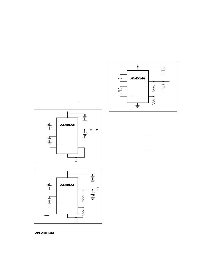
�Figure� 2c.� MAX853� Standard� Application� Circuit�
�IN�
�C3�
�1� μ� F�
�For� the� MAX853,� set� the� output� voltage,� VOUT,� by� con-�
�MAX851�
�?� R1� ?�
�C1�
�1� μ� F�
�C2�
�1� μ� F�
�C1+�
�MAX850�
�C1-�
�MAX852�
�NEGOUT�
�OUT�
�V� OUT� =� -4.1V�
�(V� GG� of� GaAsFET)�
�C4�
�10� μ� F�
�necting� a� resistor� voltage� divider� between� OUT� and� a�
�positive� control� voltage,� V� CTRL� (Figure� 2c.)�
�?� R2� ?�
�V� OUT� =� -� V� CTRL� ?� ?�
�Shutdown�
�The� MAX850–MAX853� feature� a� shutdown� mode� that�
�*MAX850:� SHDN�
�MAX851:� SHDN�
�MAX852:� OSC�
�SHDN*�
�SHDN�
�OSC�
�GND�
�FB�
�reduces� the� supply� current� to� 1μA� max� over� temperature�
�(5μA� max� for� the� MAX851).� The� MAX850� and� MAX853� have�
�an� active-low� TTL� logic� level� SHDN� input,� whereas� the�
�MAX851� has� an� active-high� SHDN� input.� To� shut� down� the�
�MAX852,� set� the� OCSC� input� to� a� logic-low� level.� The� device�
�is� powered� up� by� the� resumption� of� the� clock� signal.�
�Figure� 2a.� MAX850/MAX851/MAX852� Standard� Application� Circuit�
�V� IN�
�Capacitors�
�Use� capacitors� with� low� effective� series� resistance� (ESR)� to�
�maintain� a� low� dropout� voltage� (V� IN� -� |� V� OUT� |� ).� The� overall�
�MAX851�
�(�
�C1�
�1� μ� F�
�C2�
�1� μ� F�
�IN�
�C1+�
�MAX850�
�C1-�
�MAX852�
�NEGOUT�
�OUT�
�C3�
�1� μ� F�
�V� OUT� =� (-1.28V)� 1+� R2�
�R1�
�C4�
�10� μ� F�
�R2�
�100k�
�)�
�dropout� voltage� is� a� function� of� the� charge� pump’s� output�
�resistance� and� the� voltage� drop� across� the� linear� regulator�
�(N-channel� pass� transistor).� At� the� 100kHz� switching� fre-�
�quency,� the� charge-pump� output� resistance� is� a� function� of�
�C1� and� C2’s� ESR.� Therefore,� minimizing� the� ESR� of� the�
�charge-pump� capacitors� minimizes� the� dropout� voltage.�
�1μF,� 0.8� ?� ESR� capacitors� are� recommended� for� C1,� C2,�
�and� C3.� C4� should� be� 10μF,� 0.2� ?� ESR.� All� capacitors�
�SHDN*�
�should� be� either� surface-mount� chip� tantalum� or� chip�
�SHDN�
�OSC�
�GND�
�FB�
�R1�
�100k�
�ceramic� types.� External� capacitor� values� may� be� adjusted� to�
�optimize� size� and� cost.�
�*MAX850:� SHDN�
�MAX851:� SHDN�
�MAX852:� OSC�
�Figure� 2b.� MAX850/MAX851/MAX852� Adjustable� Configuration�
�Switching-Frequency� Control�
�Use� the� MAX852� to� minimize� system� interference� caused� by�
�conflicting� clock� frequencies.� An� external� oscillator� can� set�
�the� charge-pump� frequency� and� reduce� clock� frequency�
�_______________________________________________________________________________________�
�7�
�相关PDF资料 |
PDF描述 |
|---|---|
| MAX8530ETTG2+T | IC REG LDO 3/1.8V .2A/.15A 6TDFN |
| MAX8532EBTJ+T | IC REG LDO 2.85V .2A 6-UCSP |
| MAX8536EUA+ | IC CNTRLR ORING MOSFET 8-MSOP |
| MAX8539EEI+ | IC CNTRLR BUCK DUAL 28-QSOP |
| MAX8540EEE+T | IC REG CTRLR PWM CM 16-QSOP |
相关代理商/技术参数 |
参数描述 |
|---|---|
| MAX852ISA | 功能描述:电荷泵 RoHS:否 制造商:Maxim Integrated 功能:Inverting, Step Up 输出电压:- 1.5 V to - 5.5 V, 3 V to 11 V 输出电流:100 mA 电源电流:1 mA 最大工作温度:+ 70 C 封装 / 箱体:SOIC-8 Narrow 封装:Tube |
| MAX852ISA-T | 功能描述:电荷泵 RoHS:否 制造商:Maxim Integrated 功能:Inverting, Step Up 输出电压:- 1.5 V to - 5.5 V, 3 V to 11 V 输出电流:100 mA 电源电流:1 mA 最大工作温度:+ 70 C 封装 / 箱体:SOIC-8 Narrow 封装:Tube |
| MAX8530EB | 制造商:Rochester Electronics LLC 功能描述: 制造商:Maxim Integrated Products 功能描述: |
| MAX8530EBT2P | 制造商:Rochester Electronics LLC 功能描述: 制造商:Maxim Integrated Products 功能描述: |
| MAX8530EBT8A | 制造商:Maxim Integrated Products 功能描述:- Rail/Tube |
发布紧急采购,3分钟左右您将得到回复。