- 您现在的位置:买卖IC网 > PDF目录13559 > MAX861ESA/V+ (Maxim Integrated Products)IC REG SWITCHD CAP DBL INV 8SOIC PDF资料下载
参数资料
| 型号: | MAX861ESA/V+ |
| 厂商: | Maxim Integrated Products |
| 文件页数: | 6/11页 |
| 文件大小: | 0K |
| 描述: | IC REG SWITCHD CAP DBL INV 8SOIC |
| 产品培训模块: | Lead (SnPb) Finish for COTS Obsolescence Mitigation Program |
| 标准包装: | 100 |
| 类型: | 切换式电容器(充电泵),倍增器,反相 |
| 输出类型: | 可调式 |
| 输出数: | 1 |
| 输出电压: | -1.5 V ~ -5.5 V,5 V ~ 11 V |
| 输入电压: | 1.5 V ~ 5.5 V |
| 频率 - 开关: | 13kHz,100kHz,250kHz |
| 电流 - 输出: | 50mA |
| 同步整流器: | 无 |
| 工作温度: | -40°C ~ 85°C |
| 安装类型: | 表面贴装 |
| 封装/外壳: | 8-SOIC(0.154",3.90mm 宽) |
| 包装: | 管件 |
| 供应商设备封装: | 8-SOIC |
�� �
�
�MAX860/MAX861�
�50mA,� Frequency-Selectable,�
�Switched-Capacitor� Voltage� Converters�
�_______________Detailed� Description�
�The� MAX860/MAX861� capacitive� charge� pumps� either�
�invert� or� double� the� voltage� applied� to� their� inputs.� For�
�highest� performance,� use� low� equivalent� series� resis-�
�tance� (ESR)� capacitors.� See� the� Capacitor� Selection�
�section� for� more� details.� The� frequency-control� (FC)� pin�
�allows� you� to� choose� one� of� three� switching� frequen-�
�cies;� these� three� selectable� frequencies� are� different� for�
�each� device.� When� shut� down,� MAX860/MAX861� cur-�
�rent� consumption� reduces� to� less� than� 1μA.�
�Common� Applications�
�Voltage� Inverter�
�The� most� common� application� for� these� devices� is� a�
�charge-pump� voltage� inverter� (see� Typical� Operating�
�Circuits).� This� application� requires� only� two� external� com-�
�ponents—capacitors� C1� and� C2—plus� a� bypass� capacitor�
�if� necessary� (see� Bypass� Capacitor� section).� Refer� to� the�
�Capacitor� Selection� section� for� suggested� capacitor� types�
�and� values.�
�Even� though� the� MAX860/MAX861’s� output� is� not� actively�
�regulated,� it� is� fairly� insensitive� to� load-current� changes.� A�
�circuit� output� source� resistance� of� 12� Ω� (calculated� using�
�the� formula� given� in� the� Capacitor� Selection� section)�
�means� that,� with� a� +5V� input,� the� output� voltage� is� -5V�
�is� not� used.� When� the� device� is� shut� down,� all� active�
�circuitry� is� turned� off.�
�In� the� inverting� configuration,� loads� connected� from�
�OUT� to� GND� are� not� powered� in� shutdown� mode.�
�However,� a� reverse-current� path� exists� through� two�
�diodes� between� OUT� and� GND;� therefore,� loads� con-�
�nected� from� V� DD� to� OUT� draw� current� from� the� input�
�supply.�
�In� the� doubling� configuration,� loads� connected� from� the�
�V� DD� pin� to� the� GND� pin� are� not� powered� in� shutdown�
�mode.� Loads� connected� from� the� V� DD� pin� to� the� OUT�
�pin� draw� current� from� the� input� supply� through� a� path�
�similar� to� that� of� the� inverting� configuration� (described�
�above).�
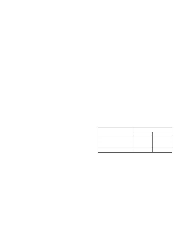
�Frequency� Control�
�Charge-pump� frequency� for� both� devices� can� be� set� to�
�one� of� three� values.� Each� device� has� a� unique� set� of�
�three� available� frequencies,� as� indicated� in� Table� 1.�
�The� oscillator� and� charge-pump� frequencies� are� the�
�same� (i.e.,� the� charge-pump� frequency� is� not� half� the�
�oscillator� frequency,� as� it� is� on� the� MAX660,� MAX665,�
�and� ICL7660).�
�Table� 1.� Nominal� Switching� Frequencies*�
�under� no� load� and� decreases� to� -4.4V� with� a� 50mA� load.�
�The� MAX860/MAX861� output� source� resistance� (used� to�
�calculate� the� circuit� output� source� resistance)� vs.� tempera-�
�FC� CONNECTION�
�FREQUENCY� (kHz)�
�MAX860� MAX861�
�ture� and� supply� voltage� are� shown� in� the� Typical�
�Operating� Characteristics� graphs.�
�Calculate� the� output� ripple� voltage� using� the� formula�
�given� in� the� Capacitor� Selection� section.�
�FC� =� V� DD� or� open�
�FC� =� GND�
�FC� =� OUT�
�6�
�50�
�130�
�13�
�100�
�250�
�Active-Low� Shutdown� Input�
�device.� In� inverter� mode,� connect� S� H� –� —� —� —� –� to� V� DD� if� it� is�
�Positive Voltage Doubler�
�The� MAX860/MAX861� can� also� operate� as� positive� volt-�
�age� doublers� (see� Typical� Operating� Circuits� ).� This�
�application� requires� only� two� external� components,�
�capacitors� C1� and� C2.� The� no-load� output� is� twice� the�
�input� voltage.� The� electrical� specifications� in� the� doubler�
�mode� are� very� similar� to� those� of� the� inverter� mode�
�except� for� the� Supply� Voltage� Range� (see� Electrical�
�Characteristics� table)� and� No-Load� Supply� Current� (see�
�graph� in� Typical� Operating� Characteristics).� The� circuit�
�output� source� resistance� and� output� ripple� voltage� are�
�calculated� using� the� formulas� in� the� Capacitor� Selection�
�section.�
�–� —� —� —� –�
�–— —–�
�When� driven� low,� the� S� H� D� N� input� —� shuts� down� the�
�D� N�
�not� used.� In� doubler� mode,� connect� S� H� D� N� to� GND� if� it�
�6�
�*See� the� Electrical� Characteristics� for� detailed� switching-�
�frequency� specifications.�
�A� higher� switching� frequency� minimizes� capacitor� size�
�for� the� same� performance� and� increases� the� supply�
�current� (Table� 2).� The� lowest� fundamental� frequency� of�
�the� switching� noise� is� equal� to� the� minimum� specified�
�switching� frequency� (e.g.,� 3kHz� for� the� MAX860� with� FC�
�open).� The� spectrum� of� noise� frequencies� extends�
�above� this� value� because� of� harmonics� in� the� switching�
�waveform.� To� get� best� noise� performance,� choose� the�
�device� and� FC� connection� to� select� a� minimum� switch-�
�ing� frequency� that� lies� above� your� sensitive� bandwidth.�
�Low-Voltage-Operation� Input�
�LV� should� be� connected� to� GND� for� inverting� operation.�
�To� enhance� compatibility� with� the� MAX660,� MAX665,� and�
�ICL7660,� you� may� float� LV� if� the� input� voltage� exceeds� 3V.�
�In� doubling� mode,� LV� must� be� connected� to� OUT� for� all�
�input� voltages.�
�Maxim� Integrated�
�相关PDF资料 |
PDF描述 |
|---|---|
| MAX750ACSA+T | IC REG BUCK ADJ 0.45A 8SOIC |
| AVS336M25C12T-F | CAP ALUM 33UF 25V 20% SMD |
| RCM22DRMI-S288 | CONN EDGECARD 44POS .156 EXTEND |
| MAX730ACSA+T | IC REG BUCK 5V 0.45A 8SOIC |
| MAX763ACSA+T | IC REG BUCK 3.3V 0.5A 8SOIC |
相关代理商/技术参数 |
参数描述 |
|---|---|
| MAX861ISA | 功能描述:电荷泵 50mA f-Selectable Switched-Cap V Conv RoHS:否 制造商:Maxim Integrated 功能:Inverting, Step Up 输出电压:- 1.5 V to - 5.5 V, 3 V to 11 V 输出电流:100 mA 电源电流:1 mA 最大工作温度:+ 70 C 封装 / 箱体:SOIC-8 Narrow 封装:Tube |
| MAX861ISA+ | 功能描述:电荷泵 50mA f-Selectable Switched-Cap V Conv RoHS:否 制造商:Maxim Integrated 功能:Inverting, Step Up 输出电压:- 1.5 V to - 5.5 V, 3 V to 11 V 输出电流:100 mA 电源电流:1 mA 最大工作温度:+ 70 C 封装 / 箱体:SOIC-8 Narrow 封装:Tube |
| MAX861ISA+T | 功能描述:电荷泵 50mA f-Selectable Switched-Cap V Conv RoHS:否 制造商:Maxim Integrated 功能:Inverting, Step Up 输出电压:- 1.5 V to - 5.5 V, 3 V to 11 V 输出电流:100 mA 电源电流:1 mA 最大工作温度:+ 70 C 封装 / 箱体:SOIC-8 Narrow 封装:Tube |
| MAX861ISA-T | 功能描述:电荷泵 50mA f-Selectable Switched-Cap V Conv RoHS:否 制造商:Maxim Integrated 功能:Inverting, Step Up 输出电压:- 1.5 V to - 5.5 V, 3 V to 11 V 输出电流:100 mA 电源电流:1 mA 最大工作温度:+ 70 C 封装 / 箱体:SOIC-8 Narrow 封装:Tube |
| MAX861ISA-TG069 | 制造商:Rochester Electronics LLC 功能描述: 制造商:Maxim Integrated Products 功能描述: |
发布紧急采购,3分钟左右您将得到回复。