- 您现在的位置:买卖IC网 > PDF目录5062 > MAX8805YEWEBE+T (Maxim Integrated Products)IC CONV STP-DN PWM 600MA 16WLP PDF资料下载
参数资料
| 型号: | MAX8805YEWEBE+T |
| 厂商: | Maxim Integrated Products |
| 文件页数: | 14/24页 |
| 文件大小: | 0K |
| 描述: | IC CONV STP-DN PWM 600MA 16WLP |
| 产品培训模块: | Lead (SnPb) Finish for COTS Obsolescence Mitigation Program |
| 标准包装: | 2,500 |
| 应用: | 转换器,WCDMA PA 电源 |
| 输入电压: | 2.7 V ~ 5.5 V |
| 输出数: | 1 |
| 输出电压: | 0.4 V ~ 5.5 V |
| 工作温度: | -40°C ~ 85°C |
| 安装类型: | 表面贴装 |
| 封装/外壳: | 16-UFBGA,WLCSP |
| 供应商设备封装: | 16-WLP(2x2) |
| 包装: | 带卷 (TR) |
�� �
�
�600mA/650mA� PWM� Step-Down� Converters� in�
�2mm� x� 2mm� WLP� for� WCDMA� PA� Power�
�Detailed� Description�
�The� MAX8805W/MAX8805X/MAX8805Y/MAX8805Z� are�
�designed� to� dynamically� power� the� PA� in� WCDMA� and�
�NCDMA� handsets.� The� devices� contain� a� high-frequency,�
�high-efficiency� step-down� converter,� and� two� LDOs.�
�The� MAX8805Y/MAX8805Z� step-down� converters� deliver�
�over� 600mA,� while� the� MAX8805W/MAX8805X� deliver�
�over� 650mA.� The� hysteretic� PWM� control� scheme� pro-�
�vides� extremely� fast� transient� response,� while� 2MHz� and�
�4MHz� switching-frequency� options� allow� the� trade-off�
�between� efficiency� and� the� smallest� external� compo-�
�nents.� A� 60m� ?� bypass� FET� connects� the� PA� directly� to�
�the� battery� during� high-power� transmission.�
�Step-Down� Converter� Control� Scheme�
�A� hysteretic� PWM� control� scheme� ensures� high� effi-�
�ciency,� fast� switching,� fast� transient� response,� low-out-�
�put� ripple,� and� physically� tiny� external� components.�
�The� control� scheme� is� simple:� when� the� output� voltage�
�is� below� the� regulation� threshold,� the� error� comparator�
�begins� a� switching� cycle� by� turning� on� the� high-side�
�switch.� This� high-side� switch� remains� on� until� the� mini-�
�mum� on-time� expires� and� the� output� voltage� is� within�
�Step-Down� Converter� Bypass� Mode�
�During� high-power� transmission,� the� bypass� mode� con-�
�nects� IN1A� and� IN1B� directly� to� PAA� and� PAB� with� the�
�internal� 60m� ?� (typ)� bypass� FET,� while� the� step-down�
�converter� is� forced� into� 100%� duty-cycle� operation.� The�
�low� on-resistance� in� this� mode� provides� low� dropout,�
�long� battery� life,� and� high� output� current� capability.�
�Forced� and� Automatic� Bypass� Mode�
�Invoke� forced� bypass� mode� by� driving� HP� high� or�
�invoke� automatic� bypass� mode� by� applying� a� high� volt-�
�age� to� REFIN.� To� prevent� excessive� output� ripple� as�
�the� step-down� converter� approaches� dropout,� the�
�MAX8805Y/MAX8805Z� enter� bypass� mode� automatical-�
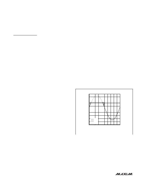
�ly� when� V� REFIN� >� 0.465� x� V� IN2� (see� Figure� 2)� and�
�MAX8805W/MAX8805X� enter� bypass� mode� automati-�
�cally� when� V� REFIN� >� 0.372� x� V� IN2� .� Note� that� IN2� is� used�
�instead� of� IN1� to� prevent� switching� noise� from� causing�
�false� enagement� of� automatic� bypass� mode.� For� this�
�reason,� IN2� must� be� connected� to� the� same� source�
�as� IN1.�
�regulation,� or� the� inductor� current� is� above� the� current-�
�limit� threshold.� Once� off,� the� high-side� switch� remains�
�off� until� the� minimum� off-time� expires� and� the� output�
�voltage� falls� again� below� the� regulation� threshold.�
�During� the� off� period,� the� low-side� synchronous� rectifier�
�turns� on� and� remains� on� until� the� high-side� switch� turns�
�on� again.� The� internal� synchronous� rectifier� eliminates�
�the� need� for� an� external� Schottky� diode.�
�Voltage-Positioning� Load� Regulation�
�5.0�
�4.5�
�4.0�
�3.5�
�3.0�
�2.5�
�2.0�
�1.5�
�2.5�
�2.0�
�1.5�
�1.0�
�The� MAX8805W/MAX8805X/MAX8805Y/MAX8805Z� step-�
�1.0�
�IN2�
�0.5�
�down� converters� utilize� a� unique� feedback� network.� By�
�taking� DC� feedback� from� the� LX� node� through� R1� in�
�Figure� 1,� the� usual� phase� lag� due� to� the� output� capacitor�
�0.5�
�0�
�0�
�5�
�PA_�
�REFIN�
�10� 15� 20� 25� 30� 35� 40� 45� 50�
�0�
�is� removed,� making� the� loop� exceedingly� stable� and�
�allowing� the� use� of� very� small� ceramic� output� capacitors.�
�To� improve� the� load� regulation,� resistor� R3� is� included� in�
�the� feedback.� This� configuration� yields� load� regulation�
�equal� to� half� of� the� inductor’s� series� resistance� multiplied�
�by� the� load� current.� This� voltage-positioning� load� regula-�
�tion� greatly� reduces� overshoot� during� load� transients� or�
�when� changing� the� output� voltage� from� one� level� to� anoth-�
�er.� However,� when� calculating� the� required� REFIN� volt-�
�age,� the� load� regulation� should� be� considered.� Because�
�inductor� resistance� is� typically� well� specified� and� the�
�typical� PA� is� a� resistive� load,� the� MAX8805Y/MAX8805Z�
�V� REFIN� to� V� OUT� gain� is� slightly� less� than� 2V/V,� and� the�
�MAX8805W/MAX8805X� V� REFIN� to� V� OUT� gain� is� slightly�
�less� than� 2.5V/V.� The� output� voltage� is� aproximately:�
�V� OUT� =� (REFIN� to� PA_Gain)� x� V� REFIN� -� 1/2� x� L� ESR� x� I� LOAD�
�TIME� (ms)�
�Figure� 2.� V� IN2� and� V� PA_� with� Automatic� Entry/Exit� into� Bypass�
�Mode� (MAX8805Y/MAX8805Z)�
�Shutdown� Mode�
�Connect� PA_EN� to� GND� or� logic-low� to� place� the�
�MAX8805W/MAX8805X/MAX8805Y/MAX8805Z� PA�
�step-down� converter� in� shutdown� mode.� In� shutdown,�
�the� control� circuitry,� internal� switching� MOSFET,� and�
�synchronous� rectifier� turn� off� and� LX� becomes� high�
�impedance.� Connect� PA_EN� to� IN1_� or� logic-high� for�
�normal� operation.�
�Connect� EN1� or� EN2� to� GND� or� logic-low� to� place�
�LDO1� or� LDO2,� respectively,� in� shutdown� mode.� In�
�14�
�______________________________________________________________________________________�
�相关PDF资料 |
PDF描述 |
|---|---|
| MAX8805ZEWEAA+T | IC CONV STP-DN PWM 600MA 16WLP |
| MAX8805YEWEGG+T | IC CONV STP-DN PWM 600MA 16WLP |
| ACC17DRAH-S734 | CONN EDGECARD 34POS .100 R/A PCB |
| MAX8805YEWECD+T | IC CONV STP-DN PWM 600MA 16WLP |
| MAX8805YEWEAA+T | IC CONV STP-DN PWM 600MA 16WLP |
相关代理商/技术参数 |
参数描述 |
|---|---|
| MAX8805YEWEBG+T | 功能描述:直流/直流开关转换器 600mA/650mA PWM Step-Down Converter RoHS:否 制造商:STMicroelectronics 最大输入电压:4.5 V 开关频率:1.5 MHz 输出电压:4.6 V 输出电流:250 mA 输出端数量:2 最大工作温度:+ 85 C 安装风格:SMD/SMT |
| MAX8805YEWECC+T | 功能描述:直流/直流开关转换器 600mA/650mA PWM Step-Down Converter RoHS:否 制造商:STMicroelectronics 最大输入电压:4.5 V 开关频率:1.5 MHz 输出电压:4.6 V 输出电流:250 mA 输出端数量:2 最大工作温度:+ 85 C 安装风格:SMD/SMT |
| MAX8805YEWECD+T | 功能描述:直流/直流开关转换器 600mA/650mA PWM Step-Down Converter RoHS:否 制造商:STMicroelectronics 最大输入电压:4.5 V 开关频率:1.5 MHz 输出电压:4.6 V 输出电流:250 mA 输出端数量:2 最大工作温度:+ 85 C 安装风格:SMD/SMT |
| MAX8805YEWECE+T | 功能描述:直流/直流开关转换器 600mA/650mA PWM Step-Down Converter RoHS:否 制造商:STMicroelectronics 最大输入电压:4.5 V 开关频率:1.5 MHz 输出电压:4.6 V 输出电流:250 mA 输出端数量:2 最大工作温度:+ 85 C 安装风格:SMD/SMT |
| MAX8805YEWEDD+T | 功能描述:直流/直流开关转换器 600mA/650mA PWM Step-Down Converter RoHS:否 制造商:STMicroelectronics 最大输入电压:4.5 V 开关频率:1.5 MHz 输出电压:4.6 V 输出电流:250 mA 输出端数量:2 最大工作温度:+ 85 C 安装风格:SMD/SMT |
发布紧急采购,3分钟左右您将得到回复。