- 您现在的位置:买卖IC网 > PDF目录20720 > MAX8862LESE+T (Maxim Integrated)IC REG LDO 4.95V/ADJ 16-SOIC PDF资料下载
参数资料
| 型号: | MAX8862LESE+T |
| 厂商: | Maxim Integrated |
| 文件页数: | 7/12页 |
| 文件大小: | 0K |
| 描述: | IC REG LDO 4.95V/ADJ 16-SOIC |
| 产品培训模块: | Lead (SnPb) Finish for COTS Obsolescence Mitigation Program |
| 标准包装: | 2,500 |
| 稳压器拓扑结构: | 正,固定式或可调式 |
| 输出电压: | 4.95V,2 V ~ 11 V |
| 输入电压: | 2.5 V ~ 11.5 V |
| 电压 - 压降(标准): | 0.16V @ 200mA,0.16V @ 100mA |
| 稳压器数量: | 2 |
| 电流 - 输出: | 250mA(最小),100mA(最小) |
| 工作温度: | -40°C ~ 85°C |
| 安装类型: | 表面贴装 |
| 封装/外壳: | 16-SOIC(0.154",3.90mm 宽) |
| 供应商设备封装: | 16-SOIC |
| 包装: | 带卷 (TR) |
�� �
�
�Low-Cost,� Low-Dropout,� Dual� Linear� Regulator�
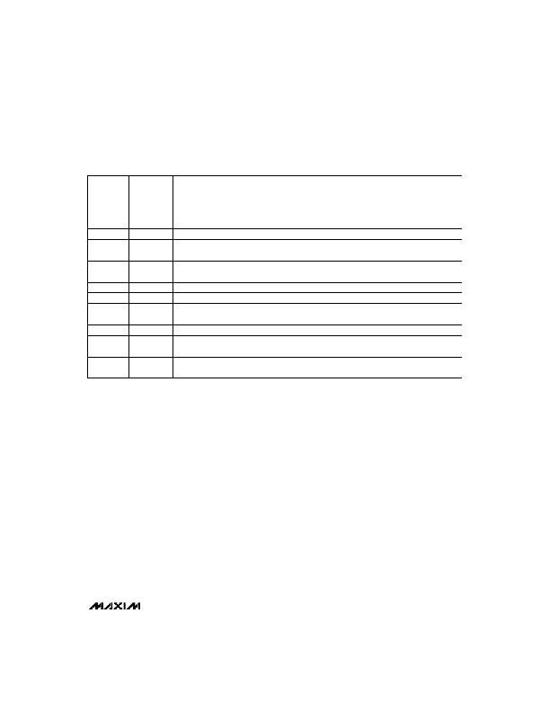
�______________________________________________________________Pin� Description�
�PIN�
�1�
�2�
�3�
�4,� 5,� 12,� 13�
�6�
�7�
�8,� 16�
�9�
�10�
�11�
�14�
�15�
�NAME�
�IN1�
�SHDN1�
�PWROK1�
�GND�
�OUT2�
�SET2�
�N.C.�
�IN2�
�SHDN2�
�REF2�
�OUT1�
�SET1�
�FUNCTION�
�Main� Regulator� Supply� Input� (2.5V� to� 11.5V).� Bypass� with� a� 1μF,� low-ESR� capacitor� to� GND.�
�Main� Regulator� Shutdown� Input.� A� logic� low� turns� off� the� main� regulator� and� power-good� comparator.�
�Power-Good� Output.� This� open-drain� output� is� low� when� V� OUT1� is� out� of� regulation� (V� OUT1� is� 4%�
�lower� than� its� nominal� value).�
�Ground.� Connect� to� a� ground� plane� to� maximize� thermal� dissipation.�
�Secondary� Regulator� Output.� Bypass� with� a� 2.2μF� low-ESR� (<� 0.5� ?� )� capacitor� to� GND.� To� improve�
�load-transient� response� and� noise� performance,� use� a� higher-value,� lower-ESR� capacitor.�
�OUT2� Voltage-Set� Input.� Connect� to� GND� for� the� factory-preset� output� voltage.� Connect� to� a� resistive�
�divider� from� OUT2� to� GND� for� adjustable� output� voltage.�
�No� connect.� There� is� no� internal� connection� to� this� pin.�
�Secondary� Regulator� Supply� Input� (2.5V� to� 11.5V).� Bypass� with� a� 1μF,� low-ESR� capacitor� to� GND.�
�Secondary� Regulator� Shutdown� Input.� A� logic-low� input� turns� off� the� secondary� regulator� and� the�
�reference.�
�Secondary� Reference� Output.� Bypass� with� a� 0.1μF� capacitor� to� GND.�
�Main� Regulator� Output.� Bypass� with� a� 3.3μF,� low-ESR� (<� 0.5� ?� )� capacitor� to� GND.� To� improve� load-�
�transient� response� and� noise� performance,� use� a� higher-value,� lower-ESR� capacitor.�
�OUT1� Voltage� Set� Input.� Connect� to� GND� for� the� factory-preset� output� voltage.� Connect� to� a�
�resistive� divider� from� OUT1� to� GND� for� adjustable� output� voltage.�
�_______________Detailed� Description�
�The� MAX8862� features� Dual� Mode?� operation,� allow-�
�ing� a� fixed� output� of� 4.95V� (L),� 3.175V� (T),� or� 2.85V� (R),�
�or� an� adjustable� output� from� 2V� to� 11V.� The� regulator’s�
�outputs,� OUT1� and� OUT2,� supply� 250mA� and� 100mA,�
�respectively.�
�The� block� diagram� (Figure� 1)� shows� the� contents� of�
�each� regulator.� Note� that� the� main� regulator� provides� a�
�power-good� indicator,� and� the� secondary� regulator’s�
�reference� output� voltage� is� available� at� REF2.�
�The� 1.25V� bandgap� reference� is� connected� to� the� error�
�amplifier’s� inverting� input.� The� error� amplifier� compares�
�this� reference� with� the� selected� feedback� voltage� and�
�amplifies� the� difference.� The� MOSFET� driver� reads� the�
�error� signal� and� applies� the� appropriate� drive� to� the�
�P-channel� transistor.� If� the� feedback� voltage� is� lower�
�than� the� reference,� the� pass� transistor’s� gate� is� pulled�
�lower,� allowing� more� current� to� pass� and� increase� the�
�output� voltage.� If� the� feedback� voltage� is� too� high,� the�
�pass� transistor’s� gate� is� pulled� up,� allowing� less� current�
�to� pass� to� the� output.�
�The� output� voltage� is� fed� back� through� either� an�
�internal� resistor� voltage� divider� connected� to� OUT1/�
�OUT2,� or� an� external� resistor� network� connected� to�
�SET1/SET2.� The� Dual� Mode� comparator� examines�
�V� SET1� /V� SET2� and� selects� the� feedback� path.� If� this� volt-�
�age� is� below� 40mV,� internal� feedback� is� used� and� the�
�output� voltage� is� regulated� to� the� factory-preset� volt-�
�age.�
�Internal� P-Channel� Pass� Transistor�
�The� MAX8862� ’s� P-channel� pass� transistor� provides�
�several� advantages� over� similar� designs� using� PNP�
�pass� transistors,� including� longer� battery� life.�
�The� P-channel� MOSFET� requires� no� continuous� base�
�current,� thereby� reducing� quiescent� current� consider-�
�ably.� PNP� regulators� normally� waste� a� considerable�
�amount� of� current� in� dropout� when� the� pass� transistor�
�saturates;� they� also� use� high� base-drive� currents� under�
�large� loads.� The� MAX8862� does� not� suffer� from� these�
�problems:� it� consumes� only� 200μA� of� quiescent� current�
�for� both� regulators� under� light� and� heavy� loads,� as� well�
�as� in� dropout.�
�_______________________________________________________________________________________�
�7�
�相关PDF资料 |
PDF描述 |
|---|---|
| MAX8559ETAAK+T | IC REG LDO 3.3V/2.8V .3A 8-TDFN |
| MAX8559ETADK+T | IC REG LDO 3.15V/2.8V .3A 8-TDFN |
| MAX8559ETA88+T | IC REG LDO 1.5V .3A 8-TDFN |
| RGM06DRMH | CONN EDGECARD 12POS .156 WW |
| HSM44DSXN | CONN EDGECARD 88POS DIP .156 SLD |
相关代理商/技术参数 |
参数描述 |
|---|---|
| MAX8862RCSE | 制造商:Rochester Electronics LLC 功能描述: 制造商:Maxim Integrated Products 功能描述: |
| MAX8862RESE | 功能描述:低压差稳压器 - LDO RoHS:否 制造商:Texas Instruments 最大输入电压:36 V 输出电压:1.4 V to 20.5 V 回动电压(最大值):307 mV 输出电流:1 A 负载调节:0.3 % 输出端数量: 输出类型:Fixed 最大工作温度:+ 125 C 安装风格:SMD/SMT 封装 / 箱体:VQFN-20 |
| MAX8862RESE+ | 功能描述:低压差稳压器 - LDO Dual Linear Regulator RoHS:否 制造商:Texas Instruments 最大输入电压:36 V 输出电压:1.4 V to 20.5 V 回动电压(最大值):307 mV 输出电流:1 A 负载调节:0.3 % 输出端数量: 输出类型:Fixed 最大工作温度:+ 125 C 安装风格:SMD/SMT 封装 / 箱体:VQFN-20 |
| MAX8862RESE+T | 功能描述:低压差稳压器 - LDO Dual Linear Regulator RoHS:否 制造商:Texas Instruments 最大输入电压:36 V 输出电压:1.4 V to 20.5 V 回动电压(最大值):307 mV 输出电流:1 A 负载调节:0.3 % 输出端数量: 输出类型:Fixed 最大工作温度:+ 125 C 安装风格:SMD/SMT 封装 / 箱体:VQFN-20 |
| MAX8862RESE-T | 功能描述:低压差稳压器 - LDO RoHS:否 制造商:Texas Instruments 最大输入电压:36 V 输出电压:1.4 V to 20.5 V 回动电压(最大值):307 mV 输出电流:1 A 负载调节:0.3 % 输出端数量: 输出类型:Fixed 最大工作温度:+ 125 C 安装风格:SMD/SMT 封装 / 箱体:VQFN-20 |
发布紧急采购,3分钟左右您将得到回复。