- 您现在的位置:买卖IC网 > PDF目录22322 > MAX8884ZEREKE+T (Maxim Integrated)IC REG TRPL BCK/LINEAR 16UCSP PDF资料下载
参数资料
| 型号: | MAX8884ZEREKE+T |
| 厂商: | Maxim Integrated |
| 文件页数: | 9/17页 |
| 文件大小: | 579K |
| 描述: | IC REG TRPL BCK/LINEAR 16UCSP |
| 产品培训模块: | Lead (SnPb) Finish for COTS Obsolescence Mitigation Program |
| 标准包装: | 2,500 |
| 拓扑: | 降压(降压)同步(1),线性(LDO)(2) |
| 功能: | 任何功能 |
| 输出数: | 3 |
| 频率 - 开关: | 4MHz |
| 电压/电流 - 输出 1: | 1.2 V/1.8 V,700mA |
| 电压/电流 - 输出 2: | 1.2 V/1.8 V,300mA |
| 电压/电流 - 输出 3: | 1.2 V/1.8 V,300mA |
| 带 LED 驱动器: | 无 |
| 带监控器: | 无 |
| 带序列发生器: | 无 |
| 电源电压: | 2.7 V ~ 5.5 V |
| 工作温度: | -40°C ~ 85°C |
| 安装类型: | 表面贴装 |
| 封装/外壳: | 16-WFBGA,CSPBGA |
| 供应商设备封装: | 16-UCSP(4x4) |
| 包装: | 带卷 (TR) |
700mA DC-DC Step-Down Converters
with Dual 300mA LDO in 2mm x 2mm CSP
_______________________________________________________________________________________ 9
Detailed Description
The MAX8884Y/MAX8884Z are designed to power the
subcircuits within a system. These ICs contain a high-
frequency, high-efficiency step-down converter and two
LDOs. The step-down converter delivers 700mA with
either 1.2V or 1.8V selectable output voltage using SEL.
The hysteretic PWM control scheme provides extremely
fast transient response, while 2MHz and 4MHz switch-
ing frequency options allow the trade-off between effi-
ciency and the smallest external components. The
MAX8884Y/MAX8884Z linear regulators can be used to
power loads requiring a low output noise supply.
Step-Down Converter Control Scheme
A hysteretic PWM control scheme ensures high efficien-
cy, fast switching, fast transient response, low-output
voltage ripple, and physically tiny external components.
The control scheme is simple: when the output voltage
is below the regulation threshold, the error comparator
begins a switching cycle by turning on the high-side
switch. This high-side switch remains on until the mini-
mum on-time expires and output voltage is within regu-
lation, or the inductor current is above the current-limit
threshold. Once off, the high-side switch remains off
until the minimum off-time expires and the output volt-
age falls again below the regulation threshold. During
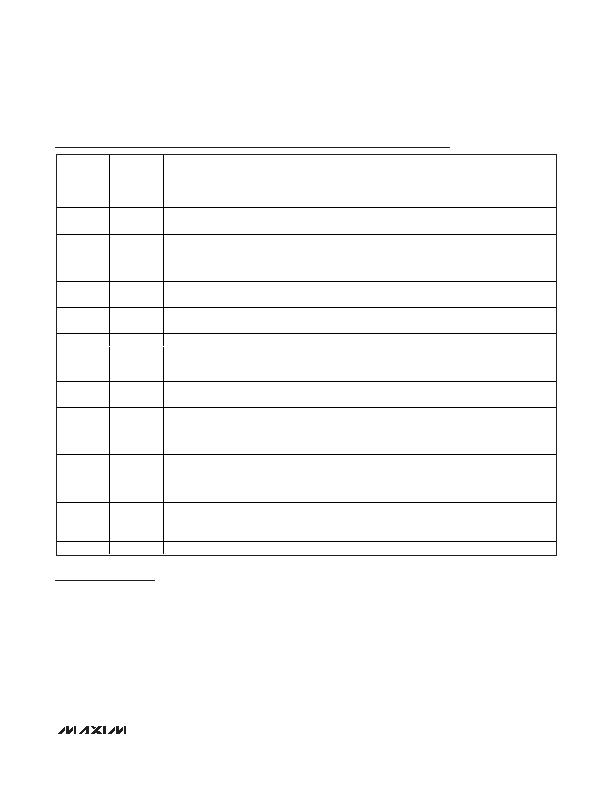
Pin Description
PIN
NAME
FUNCTION
A1
REFBP
Reference Noise Bypass. Bypass REFBP to AGND with a 0.033礔 ceramic capacitor to reduce noise
on the LDO outputs. REFBP is internally pulled to ground through a 1k& resistor during shutdown.
A2
AGND Low-Noise Analog Ground. Connect to common ground plane.
A3
NC1 No Internal Connection. Connect NC1 to ground.
A4
PGND Power Ground for Step-Down Converter. Connect to common ground plane.
B1
LDO2
300mA LDO Regulator 2 Output. For 300mA application, bypass LDO2 with a 2.2礔 ceramic capacitor
as close as possible to LDO2 and AGND. For low-output current capability, up to 10mA, an output
capacitor of 0.1礔 is sufficient to keep the output voltage stable. LDO2 is internally pulled to ground
through a 100& resistor when this regulator is disabled.
B2 BUCK_EN
Step-Down Converter Enable Input. Connect BUCK_EN to IN1_ or logic-high for normal operation.
Connect BUCK_EN to AGND or logic-low for step-down shutdown mode.
B3 LDO2_EN
LDO2 Enable Input. Connect LDO2_EN to IN2 or logic-high for normal operation. Connect LDO2_EN to
AGND or logic-low for LDO2 shutdown mode.
B4
LX Inductor Connection. Connect an inductor from LX to the output of the step-down converter.
C1
IN2
Supply Voltage Input for LDO1, LDO2, and Internal Reference. Connect IN2 to a battery or supply
voltage from 2.7V to 5.5V. Bypass IN2 with a 4.7礔 ceramic capacitor as close as possible to IN2 and
AGND. Connect IN2 to the same source as IN1A and IN1B.
C2
SEL
Output Voltage Selection for LDO1 and Step-Down Converter. Connect to IN1_ or AGND for output
voltage selection. See Table 1.
C3, C4 IN1B, IN1A
Supply Voltage Input for Step-Down Converter. Connect IN1B and IN1A to a battery or supply voltage
from 2.7V to 5.5V. Bypass the connection of IN1B and IN1A with a 2.2礔 ceramic capacitor as close as
possible to IN1B, IN1A, and PGND. IN1A
and IN1B are internally connected together. Connect IN1A
and IN1B to the same source as IN2.
D1
LDO1
300mA LDO Regulator 1 Output. For 300mA application, bypass LDO1 with a 2.2礔 ceramic capacitor
as close as possible to LDO1 and AGND. For low-output current capability, up to 10mA, an output
capacitor of 0.1礔 is sufficient to keep output voltage stable. LDO1 is internally pulled to AGND
through a 100& resistor when this regulator is disabled.
D2 LDO1_EN
LDO1 Enable Input. Connect LDO1_EN to IN2 or logic-high for normal operation. Connect LDO1_EN to
AGND or logic-low for LDO1 shutdown mode.
D3
NC2 No Internal Connection. Connect NC2 to ground.
D4
FB FB is Connected to the Internal Feedback Network
相关PDF资料 |
PDF描述 |
|---|---|
| RCC17DCMH-S288 | CONN EDGECARD 34POS .100 EXTEND |
| MCZ33998EG | IC REG CHARGEPUMP/LINEAR 24SOIC |
| ISL9440BIRZ | IC REG QD BCK/LINEAR SYNC 32-QFN |
| ISL9441IRZ | IC REG QD BCK/LINEAR SYNC 32-QFN |
| RCC17DCMD-S288 | CONN EDGECARD 34POS .100 EXTEND |
相关代理商/技术参数 |
参数描述 |
|---|---|
| MAX8885EUK25 | 制造商:Maxim Integrated Products 功能描述:LOW-DROPOUT LINEAR REGULATORS WITH - Rail/Tube |
| MAX8885EUK25+ | 制造商:Maxim Integrated Products 功能描述: |
| MAX8885EUK25+T | 功能描述:低压差稳压器 - LDO 150mA Linear Regulator RoHS:否 制造商:Texas Instruments 最大输入电压:36 V 输出电压:1.4 V to 20.5 V 回动电压(最大值):307 mV 输出电流:1 A 负载调节:0.3 % 输出端数量: 输出类型:Fixed 最大工作温度:+ 125 C 安装风格:SMD/SMT 封装 / 箱体:VQFN-20 |
| MAX8885EUK25-T | 功能描述:低压差稳压器 - LDO 150mA Linear Regulator RoHS:否 制造商:Texas Instruments 最大输入电压:36 V 输出电压:1.4 V to 20.5 V 回动电压(最大值):307 mV 输出电流:1 A 负载调节:0.3 % 输出端数量: 输出类型:Fixed 最大工作温度:+ 125 C 安装风格:SMD/SMT 封装 / 箱体:VQFN-20 |
| MAX8885EUK26 | 制造商:Rochester Electronics LLC 功能描述: 制造商:Maxim Integrated Products 功能描述: |
发布紧急采购,3分钟左右您将得到回复。