- 您现在的位置:买卖IC网 > Datasheet目录44 > MAX8896EREE+T (Maxim Integrated)IC REG TRPL BCK/LINEAR 16UCSP Datasheet资料下载
参数资料
| 型号: | MAX8896EREE+T |
| 厂商: | Maxim Integrated |
| 文件页数: | 2/17页 |
| 文件大小: | 449K |
| 描述: | IC REG TRPL BCK/LINEAR 16UCSP |
| 产品培训模块: | Lead (SnPb) Finish for COTS Obsolescence Mitigation Program |
| 标准包装: | 1 |
| 拓扑: | 降压(降压)同步(2),线性(LDO)(1) |
| 功能: | 任何功能 |
| 输出数: | 3 |
| 频率 - 开关: | 2MHz |
| 电压/电流 - 输出 1: | 0.2 V ~ 1.7 V,700mA |
| 电压/电流 - 输出 2: | 3.1V,200mA |
| 电压/电流 - 输出 3: | 2.8V,200mA |
| 带 LED 驱动器: | 无 |
| 带监控器: | 无 |
| 带序列发生器: | 无 |
| 电源电压: | 2.7 V ~ 5.5 V |
| 工作温度: | -40°C ~ 85°C |
| 安装类型: | 表面贴装 |
| 封装/外壳: | 16-WFBGA,CSPBGA |
| 供应商设备封装: | 16-UCSP(4x4) |
| 包装: | 标准包装 |
| 其它名称: | MAX8896EREE+TDKR |
Dual PWM Step-Down Converter in a 2mm x
2mm Package for WCDMA PA and RF Power
2 _______________________________________________________________________________________
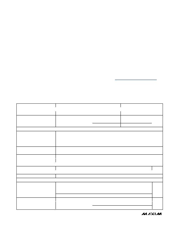
ELECTRICAL CHARACTERISTICS
(V
CC
= V
IN1
= V
IN2
= V
PAEN
= V
RFEN1
= V
RFEN2
= 3.6V, V
REFIN
= 0.72V, T
A
= -40癈 to +85癈, typical values are at T
A
= +25癈,
unless otherwise noted.) (Note 2)
Stresses beyond those listed under
Absolute Maximum Ratings
may cause permanent damage to the device. These are stress ratings only, and functional
operation of the device at these or any other conditions beyond those indicated in the operational sections of the specifications is not implied. Exposure to
absolute maximum rating conditions for extended periods may affect device reliability.
PARAMETER
CONDITIONS
MIN TYP MAX UNITS
INPUT SUPPLY
Input Voltage
V
CC
, V
IN1,
V
IN2
2.7
5.5 V
Input Undervoltage Threshold V
CC
rising, 180mV typical hysteresis
2.52 2.63
2.70 V
T
A
= +25癈
0.1
4
Shutdown Supply Current
V
P AE N
= V
R FE N 1
=
V
R FE N
2
= 0
T
A
= +85癈
0.1
礎
LOGIC CONTROL
PAEN, RFEN1, RFEN2 Logic
Input High Voltage
2.7V d V
CC
d 5.5V
1.3
V
PAEN, RFEN1, RFEN2 Logic
Input Low Voltage
2.7V d V
CC
d 5.5V
0.4 V
PAEN, RFEN1, RFEN2 Internal
Pulldown Resistor
400 800 1600 k&
T
A
= +25癈
0.01 1
PAEN, RFEN1, RFEN2 Logic
Input Current
V
IL
= 0
T
A
= +85癈
0.1
礎
REFBP
REFBP Output Voltage
0礎 d IREFBP d 1礎
1.237 1.250 1.263 V
THERMAL PROTECTION
Thermal Shutdown
T
A
rising, 20癈 typical hysteresis
+160
癈
OUT1
Quiescent Supply Current
VRFEN1 = VRFEN2 = 0V, IPA = 0A,
no switching
155
礎
p-channel MOSFET switch, I
LX1
= -200mA
0.16 0.40
On-Resistance
n-channel MOSFET rectifier, I
LX1
= 500mA
0.17 0.40
&
Load Regulation
R
L
is the inductor resistance
R
L
/2
V/A
T
A
= +25癈
0.1 5
LX1 Leakage Current
V
IN1
= 5.5V, V
LX1
= 0V
T
A
= +85癈
1
礎
ABSOLUTE MAXIMUM RATINGS
V
CC
, IN1, IN2, PAEN, RFEN1, RFEN2,
REFIN, OUT2, REFBP to AGND.........................-0.3V to +6.0V
PAOUT to AGND........................................-0.3V to (V
IN1
+ 0.3V)
LDO to AGND.........................................-0.3V to (V
OUT2
+ 0.3V)
IN1, IN2 to V
CC
......................................................-0.3V to +0.3V
IN1 to IN2..............................................................-0.3V to +0.3V
PGND1, PGND2 to AGND.....................................-0.3V to +0.3V
LX1 Current.......................................................................1A
RMS
LX2 Current.......................................................................1A
RMS
IN1 and PAOUT Current....................................................1A
RMS
PAOUT, OUT2, LDO Short Circuit to PGND1,
PGND2....................................................................Continuous
Continuous Power Dissipation (T
A
= +70癈)
16-Bump UCSP (derate 12.5mW/癈 above +70癈)............1W
Junction-to-Ambient Thermal Resistance (?/DIV>
JA
) (Note 1)...96癈/W
Junction Temperature......................................................+150癈
Storage Temperature Range.............................-65癈 to +150癈
Bump Temperature (soldering, reflow) ...........................+260癈
Note 1:Package thermal resistances were obtained using the method described in JEDEC specification JESD51-7, using a four-
layer board. For detailed information on package thermal considerations, refer to www.maxim-ic.com/thermal-tutorial
.
相关PDF资料 |
PDF描述 |
|---|---|
| MC33232PG | IC PFC CONTROLLER CRM 8DIP |
| MC33260DR2G | IC PFC CONTROLLER DCM 8SOIC |
| MC33262DG | IC PFC CONTROLLER CRM 8SOIC |
| MC33368DR2G | IC PFC CONTROLLER CRM 16SOIC |
| MC33567D-1G | IC REG CTRLR DUAL OUT 8-SOIC |
相关代理商/技术参数 |
参数描述 |
|---|---|
| MAX8896EVKIT+ | 功能描述:直流/直流开关转换器 Dual PWM Step-Down Converter in a 2mm x 2mm Package for WCDMA PA and RF Power RoHS:否 制造商:STMicroelectronics 最大输入电压:4.5 V 开关频率:1.5 MHz 输出电压:4.6 V 输出电流:250 mA 输出端数量:2 最大工作温度:+ 85 C 安装风格:SMD/SMT |
| MAX8899EVKIT+ | 制造商:Maxim Integrated Products 功能描述:EVALUATION KIT FOR MAX8899 - Boxed Product (Development Kits) |
| MAX8899EWZ+ | 制造商:Maxim Integrated Products 功能描述:- Rail/Tube |
| MAX8899EWZ+T | 制造商:Maxim Integrated Products 功能描述:WCDMA/EDGE/GPRS/GSM/CDMA - Tape and Reel |
| MAX8899EWZ+TCAA | 制造商:Maxim Integrated Products 功能描述:WCDMA/EDGE/GPRS/GSM/CDMA PHONE PMIC - Rail/Tube |
发布紧急采购,3分钟左右您将得到回复。