- 您现在的位置:买卖IC网 > PDF目录10664 > MAX9022ASA+T (Maxim Integrated Products)IC COMPARATOR DUAL 8-SOIC PDF资料下载
参数资料
| 型号: | MAX9022ASA+T |
| 厂商: | Maxim Integrated Products |
| 文件页数: | 6/8页 |
| 文件大小: | 0K |
| 描述: | IC COMPARATOR DUAL 8-SOIC |
| 其它有关文件: | Automotive Product Guide |
| 产品培训模块: | Lead (SnPb) Finish for COTS Obsolescence Mitigation Program |
| 标准包装: | 2,500 |
| 类型: | 通用 |
| 元件数: | 2 |
| 输出类型: | CMOS,满摆幅,TTL |
| 电压 - 电源,单路/双路(±): | 2.5 V ~ 5.5 V,±1.25 V ~ 2.75 V |
| 电压 - 输入偏移(最小值): | 1mV @ 5V |
| 电流 - 输入偏压(最小值): | 0.003µA @ 5V |
| 电流 - 静态(最大值): | 5µA |
| CMRR, PSRR(标准): | 100dB CMRR,80dB PSRR |
| 传输延迟(最大): | 8µs |
| 磁滞: | 4mV |
| 工作温度: | -40°C ~ 125°C |
| 封装/外壳: | 8-SOIC(0.154",3.90mm 宽) |
| 安装类型: | 表面贴装 |
| 包装: | 带卷 (TR) |
MAX9021/MAX9022/MAX9024
Micropower, Ultra-Small, Single/Dual/Quad,
Single-Supply Comparators
6
_______________________________________________________________________________________
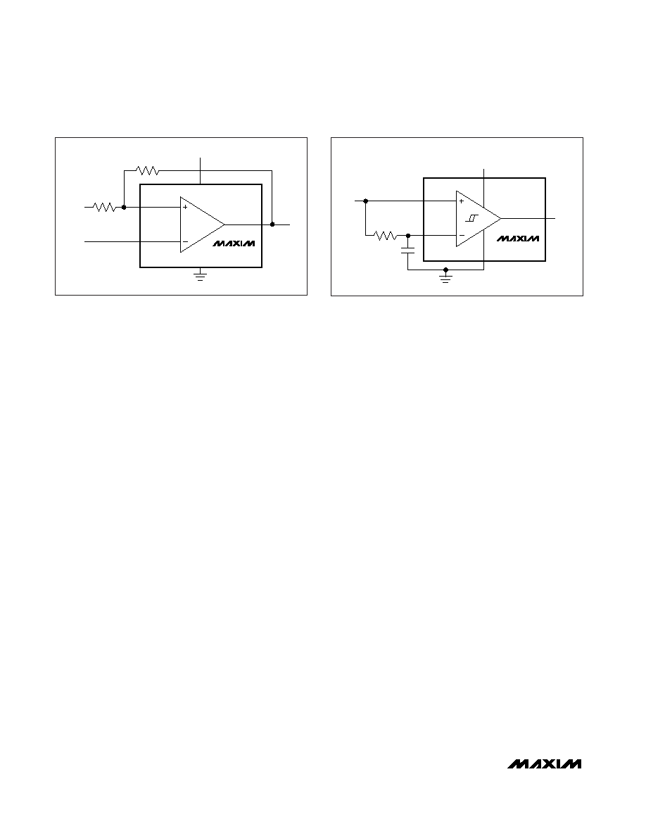
2) The hysteresis band will be:
VHYS = VTH - VTL = VDD(R2 / (R1 + R2))
3) In this example, let VDD = 5V and VREF = 2.5V.
VTH = 2.5V + 2.5V(R2 / (R1 + R2))
and
VTL = 2.5V[(1 - (R2 / (R1 + R2))]
4) Select R2. In this example, we will choose 1k
.
5) Select VHYS. In this example, we will choose 50mV.
6) Solve for R1.
VHYS = VDD(R2 / (R1 + R2))
0.050V = 5(1000
/(R1 + 1000)) V
where R1
≈ 100k, VTH = 2.525V, and VTL = 2.475V.
The above-described design procedure assumes rail-
to-rail output swing. If the output is significantly loaded,
the results should be corrected.
Board Layout and Bypassing
Use 100nF bypass as a starting point. Minimize signal
trace lengths to reduce stray capacitance. Minimize the
capacitive coupling between IN- and OUT. For slow-
moving input signals (rise time > 1ms), use a 1nF
capacitor between IN+ and IN-.
Biasing for Data Recovery
Digital data is often embedded into a bandwidth and
amplitude-limited analog path. Recovering the data can
be difficult. Figure 2 compares the input signal to a
time-averaged version of itself. This self-biases the
threshold to the average input voltage for optimal noise
margin. Even severe phase distortion is eliminated from
the digital output signal. Be sure to choose R1 and C1
so that:
fCAR >> 1 / (2
πR1C1)
where fCAR is the fundamental carrier frequency of the
digital data stream.
MAX9021
OUT
IN+
IN-
R2
R1
VIN
VREF
VDD
VSS
VDD
Figure 1. Additional Hysteresis
MAX9021
OUT
IN+
IN-
10k
0.1
F
VDD
VIN
VSS
VDD
Figure 2. Time Averaging of the Input Signal for Data Recovery
相关PDF资料 |
PDF描述 |
|---|---|
| AD9238BSTZ-20 | IC ADC 12BIT DUAL 20MSPS 64-LQFP |
| MAX9032AUA+T | IC COMPARATOR DUAL 8-UMAX |
| CS5366-DQZ | IC ADC 6CH 114DB 216KHZ 48-LQFP |
| VE-B13-MX-F1 | CONVERTER MOD DC/DC 24V 75W |
| LTC1417ACGN#PBF | IC A/D CONV 14BIT SAMPLNG 16SSOP |
相关代理商/技术参数 |
参数描述 |
|---|---|
| MAX9022AUA | 功能描述:校验器 IC Dual uPower Comparator RoHS:否 制造商:STMicroelectronics 产品: 比较器类型: 通道数量: 输出类型:Push-Pull 电源电压-最大:5.5 V 电源电压-最小:1.1 V 补偿电压(最大值):6 mV 电源电流(最大值):1350 nA 响应时间: 最大工作温度:+ 125 C 安装风格:SMD/SMT 封装 / 箱体:SC-70-5 封装:Reel |
| MAX9022AUA+ | 功能描述:校验器 IC Dual uPower Comparator RoHS:否 制造商:STMicroelectronics 产品: 比较器类型: 通道数量: 输出类型:Push-Pull 电源电压-最大:5.5 V 电源电压-最小:1.1 V 补偿电压(最大值):6 mV 电源电流(最大值):1350 nA 响应时间: 最大工作温度:+ 125 C 安装风格:SMD/SMT 封装 / 箱体:SC-70-5 封装:Reel |
| MAX9022AUA+T | 功能描述:校验器 IC Dual uPower Comparator RoHS:否 制造商:STMicroelectronics 产品: 比较器类型: 通道数量: 输出类型:Push-Pull 电源电压-最大:5.5 V 电源电压-最小:1.1 V 补偿电压(最大值):6 mV 电源电流(最大值):1350 nA 响应时间: 最大工作温度:+ 125 C 安装风格:SMD/SMT 封装 / 箱体:SC-70-5 封装:Reel |
| MAX9022AUA-T | 功能描述:校验器 IC Dual uPower Comparator RoHS:否 制造商:STMicroelectronics 产品: 比较器类型: 通道数量: 输出类型:Push-Pull 电源电压-最大:5.5 V 电源电压-最小:1.1 V 补偿电压(最大值):6 mV 电源电流(最大值):1350 nA 响应时间: 最大工作温度:+ 125 C 安装风格:SMD/SMT 封装 / 箱体:SC-70-5 封装:Reel |
| MAX9024 | 制造商:MAXIM 制造商全称:Maxim Integrated Products 功能描述:Micropower, Ultra-Small, Single/Dual/Quad, Single-Supply Comparators |
发布紧急采购,3分钟左右您将得到回复。