- 您现在的位置:买卖IC网 > PDF目录10660 > MAX9109EXT+T (Maxim Integrated Products)IC COMPAR LP SGL SC70-6 PDF资料下载
参数资料
| 型号: | MAX9109EXT+T |
| 厂商: | Maxim Integrated Products |
| 文件页数: | 7/13页 |
| 文件大小: | 0K |
| 描述: | IC COMPAR LP SGL SC70-6 |
| 产品培训模块: | Lead (SnPb) Finish for COTS Obsolescence Mitigation Program |
| 标准包装: | 1 |
| 类型: | 带锁销 |
| 元件数: | 1 |
| 输出类型: | TTL |
| 电压 - 电源,单路/双路(±): | 4.5 V ~ 5.5 V |
| 电压 - 输入偏移(最小值): | 1.6mV @ 5V |
| 电流 - 输入偏压(最小值): | 0.125µA @ 5V |
| 电流 - 静态(最大值): | 700µA |
| CMRR, PSRR(标准): | 86.02dB CMRR,86.02dB PSRR |
| 传输延迟(最大): | 25ns |
| 磁滞: | 2mV |
| 工作温度: | -40°C ~ 85°C |
| 封装/外壳: | 6-TSSOP,SC-88,SOT-363 |
| 安装类型: | 表面贴装 |
| 包装: | 标准包装 |
| 产品目录页面: | 1391 (CN2011-ZH PDF) |
| 其它名称: | MAX9109EXT+TDKR |

MAX9107/MAX9108/MAX9109
25ns, Dual/Quad/Single, Low-Power,
TTL Comparators
_______________________________________________________________________________________
3
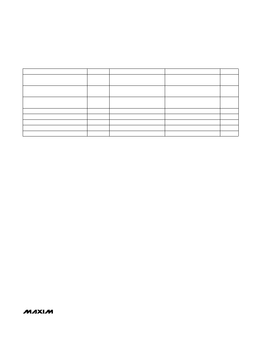
ELECTRICAL CHARACTERISTICS (continued)
(VCC = +5V, VCM = 0, VLE = 0 (MAX9109 only), TA = TMIN to TMAX, unless otherwise noted. Typical values are at TA = +25°C.) (Note 1)
Latch Hold Time
Latch Setup Time
Latch Input Current
Latch Input Voltage Low
Latch Input Voltage High
Propagation Delay Skew
Differential Propagation Delay
Propagation Delay
PARAMETER
SYMBOL
tPD+, tPD-
tPD
tPDskew
VIH
VIL
IIH, IIL
ts
th
(Note 8)
VIN = 100mV, VOD = 10mV
(Note 7)
VIN = 100mV, VOD = 10mV
(Note 6)
VIN = 100mV, VOD = 10mV
CONDITIONS
MIN
TYP
MAX
25
1
5
2.0
0.8
0.4
1
2
ns
A
V
ns
UNITS
Note 1:
Devices are 100% production tested at TA = +25°C. All temperature limits are guaranteed by design.
Note 2:
Input Offset Voltage is defined as the center of the input-referred hysteresis zone. Specified for VCM = 0. See Figure 1.
Note 3:
Trip Point is defined as the input voltage required to make the comparator output change state. The difference
between upper (VTRIP+) and lower (VTRIP-) trip points is equal to the width of the input-referred hysteresis zone (VHYST).
Specified for an input common-mode voltage (VCM) of 0. See Figure 1.
Note 4:
Inferred from the CMRR test. Note that a correct logic result is obtained at the output, provided that at least one input is
within the VCMR limits. Note also that either or both inputs can be driven to the upper or lower absolute maximum limit with-
out damage to the part.
Note 5:
Tested over the full-input voltage range (VCMR).
Note 6:
Differential Propagation Delay is specified as the difference between any two channels in the MAX9107/MAX9108 (both
outputs making either a low-to-high or a high-to-low transition).
Note 7:
Propagation Delay Skew is specified as the difference between any single channel’s output low-to-high transition (tPD+)
and high-to-low transition (tPD-).
Note 8:
Latch specifications apply to MAX9109 only. See Figure 2.
相关PDF资料 |
PDF描述 |
|---|---|
| VE-J13-MW-F4 | CONVERTER MOD DC/DC 24V 100W |
| HEW.LM.368.XLNP | CONN RCPT 68POS PNL MT SKT W/NUT |
| VE-J13-MW-F3 | CONVERTER MOD DC/DC 24V 100W |
| AD7688BRMZ | IC ADC DIFF 16BIT 500KSPS 10MSOP |
| MAX981CPA+ | IC COMPARATOR OD 8-DIP |
相关代理商/技术参数 |
参数描述 |
|---|---|
| MAX910C/D | 制造商:MAXIM 制造商全称:Maxim Integrated Products 功能描述:Analog Comparator |
| MAX910CAG | 制造商:MAXIM 制造商全称:Maxim Integrated Products 功能描述:Analog Comparator |
| MAX910CNG | 制造商:MAXIM 制造商全称:Maxim Integrated Products 功能描述:VOLT COMPARATOR|SINGLE|DIP|24PIN|PLASTIC |
| MAX910CWG | 制造商:MAXIM 制造商全称:Maxim Integrated Products 功能描述:Analog Comparator |
| MAX910EAG | 制造商:MAXIM 制造商全称:Maxim Integrated Products 功能描述:Analog Comparator |
发布紧急采购,3分钟左右您将得到回复。