参数资料
| 型号: | MAX9112ESA+T |
| 厂商: | Maxim Integrated Products |
| 文件页数: | 6/8页 |
| 文件大小: | 0K |
| 描述: | IC DRVR DUAL LVDS 8-SOIC |
| 产品培训模块: | Lead (SnPb) Finish for COTS Obsolescence Mitigation Program |
| 标准包装: | 2,500 |
| 类型: | 驱动器 |
| 驱动器/接收器数: | 2/0 |
| 规程: | LVDS |
| 电源电压: | 3 V ~ 3.6 V |
| 安装类型: | 表面贴装 |
| 封装/外壳: | 8-SOIC(0.154",3.90mm 宽) |
| 供应商设备封装: | 8-SOIC |
| 包装: | 带卷 (TR) |
MAX9110/MAX9112
Single/Dual LVDS Line Drivers with
Ultra-Low Pulse Skew in SOT23
6
_______________________________________________________________________________________
V OS
VCC
GND
DIN_
RL/2
VOS
VOD
DO_-
DO_+
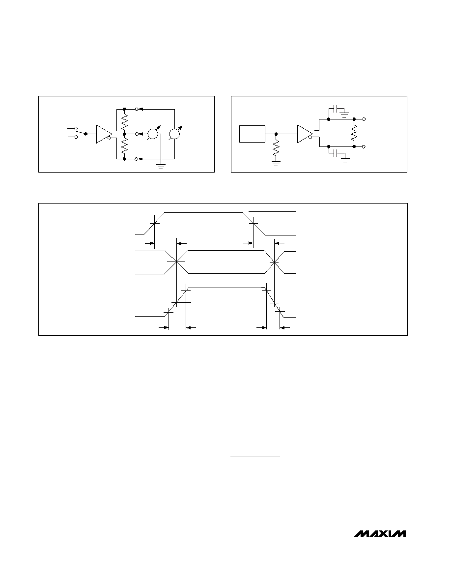
Figure 1. LVDS Transmitter VOD and VOS Test Circuit
RL
CL
DO_ +
DO_ -
CL
50
Ω
DIN_
GENERATOR
Figure 2. Transmitter Propagation Delay and Transition Time
Test Circuit
stage presents a symmetrical, high-impedance output,
reducing differential reflection and timing distortion. The
driver outputs are short circuit current limited and enter a
high-impedance state when the device is not powered.
LVDS Operation
The LVDS interface standard is a signaling method
intended for point-to-point communication over a con-
trolled impedance medium as defined by the EIA/TIA-
644 LVDS standard. The LVDS standard uses a lower
voltage swing than other common communication stan-
dards, achieving higher data rates with reduced power
consumption while reducing EMI emissions and system
susceptibility to noise.
LVDS transmitters such as the MAX9110/MAX9112
convert CMOS/LVTTL signals to low-voltage differential
signals at rates in excess of 500Mbps. The MAX9110/
MAX9112 current-steering architecture requires a resis-
tive load to terminate the signal and complete the trans-
mission loop. Because the device switches the direc-
tion of current flow and not voltage levels, the actual
output voltage swing is determined by the value of the
termination resistor at the input of an LVDS receiver.
Logic states are determined by the direction of current
flow through the termination resistor. With a typical
3.5mA output current, the MAX9110/MAX9112 produce
an output voltage of 350mV when driving a 100
Ω load.
The steady-state-voltage peak-to-peak swing is twice
the differential voltage, or 700mV (typ).
Applications Information
Supply Bypassing
Bypass VCC with high-frequency surface-mount ceramic
0.1F and 0.001F capacitors in parallel, as close to the
device as possible, with the smaller valued capacitor the
closest. For additional supply bypassing, place a 10F
tantalum or ceramic capacitor at the point where power
enters the circuit board.
0
VOH
VOL
DIN_
DO_ -
DO_+
VDIFF
3V
tPHLD
1.5V
0
tTHL
20%
0
80%
0
tTLH
20%
0V DIFFERENTIAL
tPLHD
1.5V
VDIFF = VDO_+ - VDO_-
Figure 3. Transmitter Propagation Delay and Transition Time Waveforms
相关PDF资料 |
PDF描述 |
|---|---|
| MAX9113ESA+ | IC LINE RCVR LVDS DUAL 8SOIC |
| MAX9122EUE+T | IC LINE RCVR LVDS QUAD 16TSSOP |
| MAX9123EUE+T | IC LINE DRVR LVDS QUAD 16TSSOP |
| MAX9124EUE+T | IC QUAD LVDS LINE DRIVER 16TSSOP |
| MAX9126EUE+T | IC QUAD LVDS LINE RCVR 16-TSSOP |
相关代理商/技术参数 |
参数描述 |
|---|---|
| MAX9113 | 制造商:MAXIM 制造商全称:Maxim Integrated Products 功能描述:Single/Dual LVDS Line Receivers with Ultra-Low Pulse Skew in SOT23 |
| MAX9113ASA/V+ | 制造商:Maxim Integrated Products 功能描述:- Rail/Tube |
| MAX9113ASA/V+T | 制造商:Maxim Integrated Products 功能描述:- Tape and Reel |
| MAX9113EKA | 制造商:Maxim Integrated Products 功能描述:SINGLE / DUAL LVDS LINE RECEIVER WITH ULTRA-L - Rail/Tube |
| MAX9113EKA/GH9 | 制造商:Maxim Integrated Products 功能描述:SINGLE/DUAL LVDS LINE RECEIVERS WITH ULTRA-LOW PULSE SKEW IN - Bulk |
发布紧急采购,3分钟左右您将得到回复。