- 您现在的位置:买卖IC网 > PDF目录9814 > MAX9121EUE+T (Maxim Integrated Products)IC RCVR QUAD LVDS 16-TSSOP PDF资料下载
参数资料
| 型号: | MAX9121EUE+T |
| 厂商: | Maxim Integrated Products |
| 文件页数: | 9/12页 |
| 文件大小: | 0K |
| 描述: | IC RCVR QUAD LVDS 16-TSSOP |
| 产品培训模块: | Lead (SnPb) Finish for COTS Obsolescence Mitigation Program |
| 标准包装: | 2,500 |
| 类型: | 接收器 |
| 驱动器/接收器数: | 0/4 |
| 规程: | LVDS |
| 电源电压: | 3 V ~ 3.6 V |
| 安装类型: | 表面贴装 |
| 封装/外壳: | 16-TSSOP(0.173",4.40mm 宽) |
| 供应商设备封装: | 16-TSSOP |
| 包装: | 带卷 (TR) |
MAX9121/MAX9122
Quad LVDS Line Receivers with
Integrated Termination and Flow-Through Pinout
6
_______________________________________________________________________________________
Detailed Description
The LVDS interface standard is a signaling method
intended for point-to-point communication over a con-
trolled-impedance medium as defined by the ANSI
TIA/EIA-644 and IEEE 1596.3 standards. The LVDS stan-
dard uses a lower voltage swing than other common
communication standards, achieving higher data rates
with reduced power consumption while reducing EMI
emissions and system susceptibility to noise.
The MAX9121/MAX9122 are 500Mbps, four-channel
LVDS receivers intended for high-speed, point-to-point,
low-power applications. Each channel accepts an
LVDS input and translates it to an LVTTL/LVCMOS out-
put. The receiver is capable of detecting differential
signals as low as 100mV and as high as 1V within an
input voltage range of 0 to 2.4V. The 250mV to 400mV
differential output of an LVDS driver is nominally cen-
tered around a +1.2V offset. This offset, coupled with
the receiver’s 0 to 2.4V input voltage range, allows an
approximate ±1V shift in the signal (as seen by the
receiver). This allows for a difference in ground refer-
ences of the transmitter and the receiver, the common-
mode effects of coupled noise, or both. The LVDS stan-
dards specify an input voltage range of 0 to +2.4V
referenced to receiver ground.
The MAX9122 has an integrated termination resistor
that is internally connected across each receiver input.
The internal termination saves board space, eases lay-
out, and reduces stub length compared to an external
termination resistor. In other words, the transmission
line is terminated on the IC.
Fail-Safe
The fail-safe feature of the MAX9121/MAX9122 sets an
output high when:
Inputs are open.
Inputs are undriven and shorted.
Inputs are undriven and terminated.
A fail-safe circuit is important because under these
conditions, noise at the inputs may switch the receiver
and it may appear to the system that data is being
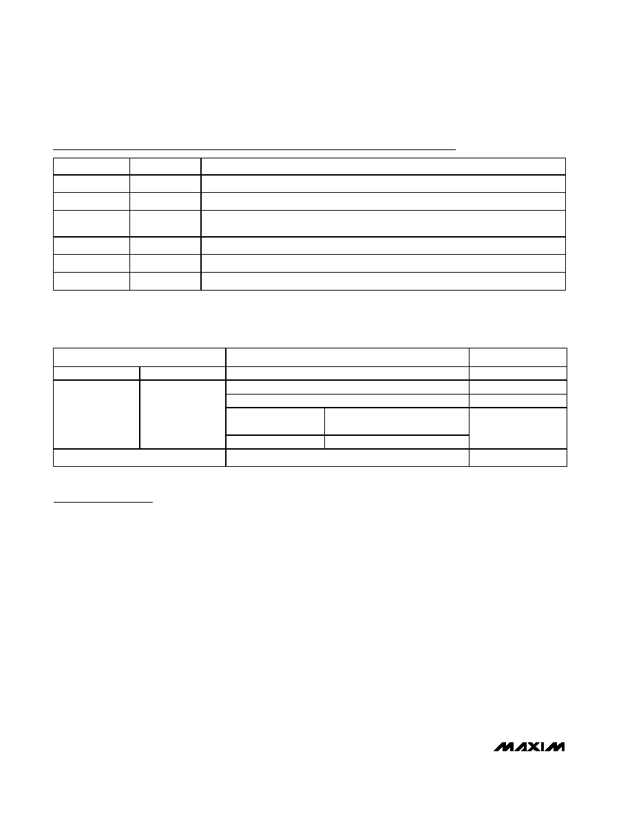
Pin Description
PIN
NAME
FUNCTION
1, 4, 5, 8
IN_-
Inverting Differential Receiver Inputs
2, 3, 6, 7
IN_+
Noninverting Differential Receiver Inputs
9, 16
EN, EN
Receiver Enable Inputs. When EN = high and
EN = low or open, the outputs are active. For
other combinations of EN and
EN, the outputs are disabled and in high impedance.
10, 11, 14, 15
OUT_
LVCMOS/LVTTL Receiver Outputs
12
GND
Ground
13
VCC
Power-Supply Input. Bypass VCC to GND with 0.1F and 0.001F ceramic capacitors.
Table 1. Input/Output Function Table
ENABLES
INPUTS
OUTPUT
EN
EN
(IN_+) - (IN_-)
OUT_
VID
≥ +100mV
H
VID
≤ -100mV
L
MAX9121
Open, undriven short, or undriven
100
parallel termination
H
L or open
MAX9122
Open or undriven short
H
All other combinations of ENABLE pins
Don’t care
Z
相关PDF资料 |
PDF描述 |
|---|---|
| VI-J6X-MX-F2 | CONVERTER MOD DC/DC 5.2V 75W |
| MAX9124ESE+T | IC DRVR QUAD LVDS 16-SOIC |
| MS27656E13B8PB | CONN RCPT 8POS WALL MNT W/PINS |
| MAX3486ESA+T | IC TXRX RS485/422 2.5MBPS 8SOIC |
| MS27497T8F98PA | CONN RCPT 3POS WALL MNT W/PINS |
相关代理商/技术参数 |
参数描述 |
|---|---|
| MAX9121EVKIT | 功能描述:LVDS 接口集成电路 Evaluation Kit for the MAX9121 MAX9122 MAX9123 RoHS:否 制造商:Texas Instruments 激励器数量:4 接收机数量:4 数据速率:155.5 Mbps 工作电源电压:5 V 最大功率耗散:1025 mW 最大工作温度:+ 85 C 封装 / 箱体:SOIC-16 Narrow 封装:Reel |
| MAX9122 | 制造商:MAXIM 制造商全称:Maxim Integrated Products 功能描述:Quad LVDS Line Receivers with Integrated Termination and Flow-Through Pinout |
| MAX9122ESE | 制造商:Maxim Integrated Products 功能描述:QUAD LVDS LINE RECEIVER WITH INTEGRATED TERMI - Bulk 制造商:Rochester Electronics LLC 功能描述: |
| MAX9122ESE+ | 制造商:Maxim Integrated Products 功能描述:LINE RCVR 4RX 16SOIC N - Bulk |
| MAX9122ESE+T | 制造商:Maxim Integrated Products 功能描述:LINE RCVR 4RX 16SOIC N - Tape and Reel |
发布紧急采购,3分钟左右您将得到回复。