- 您现在的位置:买卖IC网 > PDF目录11322 > MAX9152ESE+ (Maxim Integrated Products)IC CROSSPOINT SWITCH 2X2 16SOIC PDF资料下载
参数资料
| 型号: | MAX9152ESE+ |
| 厂商: | Maxim Integrated Products |
| 文件页数: | 12/12页 |
| 文件大小: | 0K |
| 描述: | IC CROSSPOINT SWITCH 2X2 16SOIC |
| 产品培训模块: | Lead (SnPb) Finish for COTS Obsolescence Mitigation Program |
| 标准包装: | 50 |
| 功能: | 交叉点开关 |
| 电路: | 1 x 2:2 |
| 电压电源: | 单电源 |
| 电压 - 电源,单路/双路(±): | 3 V ~ 3.6 V |
| 工作温度: | -40°C ~ 85°C |
| 安装类型: | 表面贴装 |
| 封装/外壳: | 16-SOIC(0.154",3.90mm 宽) |
| 供应商设备封装: | 16-SOIC |
| 包装: | 管件 |
lel as close to the device as possible, with the smaller
value capacitor closest to VCC.
Differential Traces
Trace characteristics affect the performance of the
MAX9152. Use controlled-impedance traces. Eliminate
reflections and ensure that noise couples as common
mode by running the differential trace pairs close
together. Reduce skew by matching the electrical
length of the traces. Excessive skew can result in a
degradation of magnetic field cancellation.
Maintain the distance between the differential traces to
avoid discontinuities in differential impedance. Avoid
90
° turns and minimize the number of vias to further
prevent impedance discontinuities.
Cables and Connectors
Transmission media should have nominal differential
impedance of 75
or 100. Use cables and connec-
tors that have matched differential impedance to mini-
mize impedance discontinuities.
Avoid the use of unbalanced cables such as ribbon or
simple coaxial cable. Balanced cables such as twisted
pair offer superior signal quality and tend to generate
less EMI due to canceling effects. Balanced cables
tend to pick up noise as common mode, which is
rejected by the differential receiver.
Board Layout
For LVDS applications, a four-layer printed-circuit (PC)
board that provides separate power, ground, and sig-
nal planes is recommended.
MAX9152
800Mbps LVDS/LVPECL-to-LVDS 2 x 2
Crosspoint Switch
_______________________________________________________________________________________
9
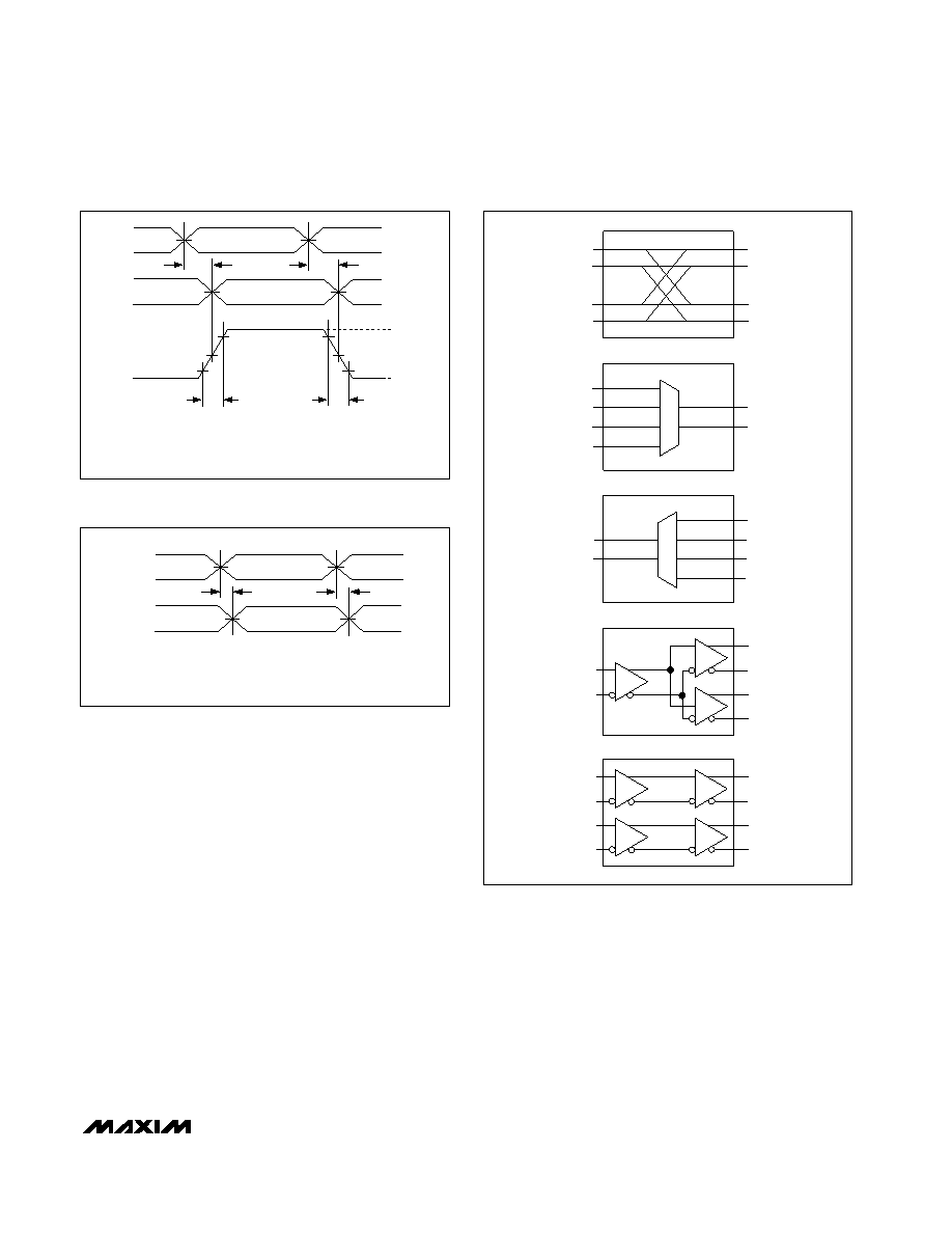
20%
50%
tPLHD AND tPHLD ARE MEASURED FOR ANY COMBINATION OF SEL0 AND SEL1.
80%
VID = (VIN_+) - (VIN_-)
VOD = (VOUT_+) - (VOUT_-)
VOD = 0
VID = 0
VOD = 0
+VOD
-VOD
tLHT
tHLT
VOUT_-
VOUT_+
VIN_-
VIN_+
tPLHD
tPHLD
Figure 6. Output Transition Time and Propagation Delay Timing
Diagram
tCCS IS MEASURED WITH SEL0 = SEL1 = HIGH OR LOW
(1:2 SPLITTER MODE)
VOD = (VOUT_+) - (VOUT_-)
VOD = 0
VOUT1-
VOUT1+
VOUT0-
VOUT0+
tCCS
Figure 7. Output Channel-to-Channel Skew
OUT0
OUT0 OR OUT1
OUT1
2 x 2 CROSSPOINT
2:1 MUX
1:2 DEMUX
1:2 SPLITTER
DUAL REPEATER
OUT0
OUT1
OUT0
OUT1
OUT0
OUT1
IN0
IN1
IN0
IN1
IN0
IN1
IN0 OR IN1
Figure 8. Programmable Configurations
相关PDF资料 |
PDF描述 |
|---|---|
| MAX4667ESE+ | IC SWITCH DUAL SPST 16SOIC |
| DG408EUE+ | IC MULTIPLEXER 8X1 16TSSOP |
| VE-JTJ-IX-F3 | CONVERTER MOD DC/DC 36V 75W |
| PIC16LC74B-04I/P | IC MCU OTP 4KX14 A/D PWM 40DIP |
| MAX383CPE+ | IC SWITCH DUAL SPDT 16DIP |
相关代理商/技术参数 |
参数描述 |
|---|---|
| MAX9152ESE+ | 功能描述:模拟和数字交叉点 IC LVDS/LVPECL-to-LVDS 2x2 Crosspoint Swtch RoHS:否 制造商:Micrel 配置:2 x 2 封装 / 箱体:MLF-16 数据速率:10.7 Gbps 输入电平:CML, LVDS, LVPECL 输出电平:CML 电源电压-最大:3.6 V 电源电压-最小:2.375 V 最大工作温度:+ 85 C 最小工作温度:- 40 C 产品:Digital Crosspoint 封装:Tube |
| MAX9152ESE+T | 功能描述:模拟和数字交叉点 IC LVDS/LVPECL-to-LVDS 2x2 Crosspoint Swtch RoHS:否 制造商:Micrel 配置:2 x 2 封装 / 箱体:MLF-16 数据速率:10.7 Gbps 输入电平:CML, LVDS, LVPECL 输出电平:CML 电源电压-最大:3.6 V 电源电压-最小:2.375 V 最大工作温度:+ 85 C 最小工作温度:- 40 C 产品:Digital Crosspoint 封装:Tube |
| MAX9152ESE-T | 功能描述:模拟和数字交叉点 IC RoHS:否 制造商:Micrel 配置:2 x 2 封装 / 箱体:MLF-16 数据速率:10.7 Gbps 输入电平:CML, LVDS, LVPECL 输出电平:CML 电源电压-最大:3.6 V 电源电压-最小:2.375 V 最大工作温度:+ 85 C 最小工作温度:- 40 C 产品:Digital Crosspoint 封装:Tube |
| MAX9152EUE | 功能描述:模拟和数字交叉点 IC RoHS:否 制造商:Micrel 配置:2 x 2 封装 / 箱体:MLF-16 数据速率:10.7 Gbps 输入电平:CML, LVDS, LVPECL 输出电平:CML 电源电压-最大:3.6 V 电源电压-最小:2.375 V 最大工作温度:+ 85 C 最小工作温度:- 40 C 产品:Digital Crosspoint 封装:Tube |
| MAX9152EUE+ | 功能描述:模拟和数字交叉点 IC LVDS/LVPECL-to-LVDS 2x2 Crosspoint Swtch RoHS:否 制造商:Micrel 配置:2 x 2 封装 / 箱体:MLF-16 数据速率:10.7 Gbps 输入电平:CML, LVDS, LVPECL 输出电平:CML 电源电压-最大:3.6 V 电源电压-最小:2.375 V 最大工作温度:+ 85 C 最小工作温度:- 40 C 产品:Digital Crosspoint 封装:Tube |
发布紧急采购,3分钟左右您将得到回复。