- 您现在的位置:买卖IC网 > PDF目录11385 > MAX9152EUE+ (Maxim Integrated Products)IC CROSSPOINT SWITCH 2X2 16TSSOP PDF资料下载
参数资料
| 型号: | MAX9152EUE+ |
| 厂商: | Maxim Integrated Products |
| 文件页数: | 10/12页 |
| 文件大小: | 0K |
| 描述: | IC CROSSPOINT SWITCH 2X2 16TSSOP |
| 产品培训模块: | Lead (SnPb) Finish for COTS Obsolescence Mitigation Program |
| 标准包装: | 96 |
| 功能: | 交叉点开关 |
| 电路: | 1 x 2:2 |
| 电压电源: | 单电源 |
| 电压 - 电源,单路/双路(±): | 3 V ~ 3.6 V |
| 工作温度: | -40°C ~ 85°C |
| 安装类型: | 表面贴装 |
| 封装/外壳: | 16-TSSOP(0.173",4.40mm 宽) |
| 供应商设备封装: | 16-TSSOP |
| 包装: | 管件 |
Input Fail-Safe
The differential inputs of the MAX9152 do not have
internal fail-safe biasing. If fail-safe biasing is required,
it can be implemented with external large-value resis-
tors. IN_+ should be pulled up to VCC with 10k
and
IN_ should be pulled down to GND with 10k
. The volt-
age-divider formed by the 10k
resistors and the 100
termination resistor (across IN_+ and IN_-) provides a
slight positive differential bias and sets a high state at
the device output when inputs are undriven.
Output Resistance
The MAX9152 has a selectable differential output resis-
tance to reduce reflections from impedance discontinu-
ities in the interconnect. Reflections are reduced,
compared to a high-impedance output. A termination
resistor at the receiver is still required and is the primary
termination for the interconnect. Select the output resis-
tance that best matches the differential characteristic
impedance of the interconnect used.
Select Function
The SEL0 and SEL1 logic inputs allow the device to be
configured as a high-speed differential crosspoint, 2:1
mux, 1:2 demux, dual repeater, or 1:2 splitter (Figure
8). See Table 1 for mode selection settings.
Enable Function
The EN0 and EN1 logic inputs enable and disable dri-
ver outputs OUT0 and OUT1. Setting EN0 or EN1 high
enables the corresponding driver output. Setting EN0
MAX9152
800Mbps LVDS/LVPECL-to-LVDS 2 x 2
Crosspoint Switch
_______________________________________________________________________________________
7
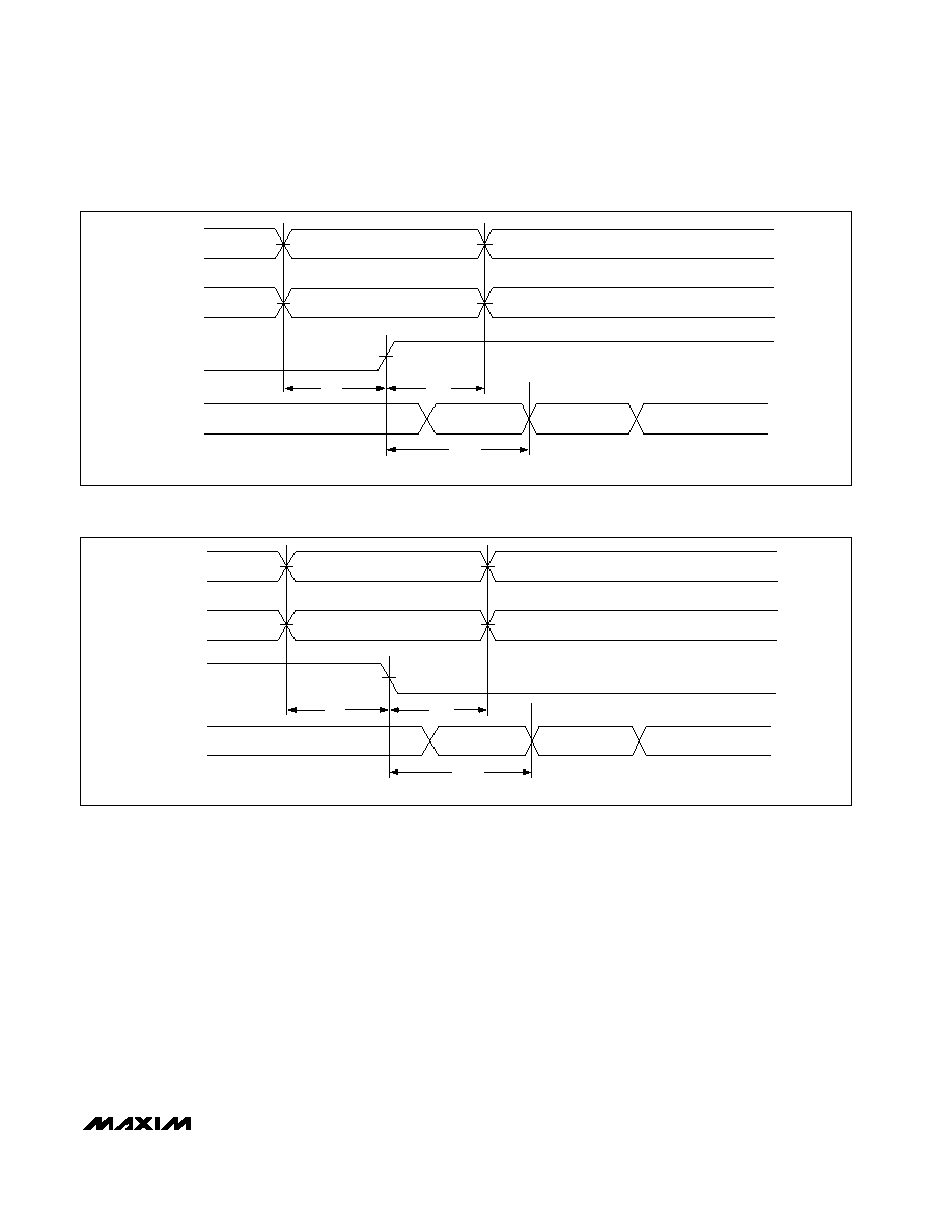
1.5V
EN0 = EN1 = HIGH
VID = (VIN_+)
(VIN_-)
tHOLD
tSWITCH
tSET
VID = 0
IN1
IN0
IN0+
IN0-
IN1-
IN1+
OUT_-
SEL_
OUT_+
1.5V
EN0 = EN1 = HIGH
VID = (VIN_+)
(VIN_-)
tHOLD
tSWITCH
tSET
VID = 0
IN0
IN1
IN0+
IN0-
IN1-
IN1+
OUT_+
SEL_
OUT_-
Figure 2. Input to Rising Edge Select Setup, Hold, and Mux Switch Timing Diagram
Figure 3. Input to Falling Edge Select Setup, Hold, and Mux Switch Timing Diagram
相关PDF资料 |
PDF描述 |
|---|---|
| IH5043CPE+ | IC SWITCH DUAL SPDT 16DIP |
| VI-B1T-IY-S | CONVERTER MOD DC/DC 6.5V 50W |
| VE-213-CU | CONVERTER MOD DC/DC 24V 200W |
| VI-25N-CU | CONVERTER MOD DC/DC 18.5V 200W |
| VI-B1W-IY-S | CONVERTER MOD DC/DC 5.5V 50W |
相关代理商/技术参数 |
参数描述 |
|---|---|
| MAX9152EUE+ | 功能描述:模拟和数字交叉点 IC LVDS/LVPECL-to-LVDS 2x2 Crosspoint Swtch RoHS:否 制造商:Micrel 配置:2 x 2 封装 / 箱体:MLF-16 数据速率:10.7 Gbps 输入电平:CML, LVDS, LVPECL 输出电平:CML 电源电压-最大:3.6 V 电源电压-最小:2.375 V 最大工作温度:+ 85 C 最小工作温度:- 40 C 产品:Digital Crosspoint 封装:Tube |
| MAX9152EUE+T | 功能描述:模拟和数字交叉点 IC LVDS/LVPECL-to-LVDS 2x2 Crosspoint Swtch RoHS:否 制造商:Micrel 配置:2 x 2 封装 / 箱体:MLF-16 数据速率:10.7 Gbps 输入电平:CML, LVDS, LVPECL 输出电平:CML 电源电压-最大:3.6 V 电源电压-最小:2.375 V 最大工作温度:+ 85 C 最小工作温度:- 40 C 产品:Digital Crosspoint 封装:Tube |
| MAX9152EUE-T | 功能描述:模拟和数字交叉点 IC RoHS:否 制造商:Micrel 配置:2 x 2 封装 / 箱体:MLF-16 数据速率:10.7 Gbps 输入电平:CML, LVDS, LVPECL 输出电平:CML 电源电压-最大:3.6 V 电源电压-最小:2.375 V 最大工作温度:+ 85 C 最小工作温度:- 40 C 产品:Digital Crosspoint 封装:Tube |
| MAX9153 | 制造商:MAXIM 制造商全称:Maxim Integrated Products 功能描述:Low-Jitter, 800Mbps, 10-Port LVDS Repeaters with 100 зDrive |
| MAX9153EUI | 制造商:Maxim Integrated Products 功能描述:LOW-JITTER, 800MBPS, 10-PORT LVDS REPEATERS W - Bulk |
发布紧急采购,3分钟左右您将得到回复。