参数资料
| 型号: | MAX9180EXT+T |
| 厂商: | Maxim Integrated Products |
| 文件页数: | 2/9页 |
| 文件大小: | 0K |
| 描述: | IC REPEATER LVDS SC70-6 |
| 产品培训模块: | Lead (SnPb) Finish for COTS Obsolescence Mitigation Program |
| 标准包装: | 1 |
| 类型: | 转发器 |
| Tx/Rx类型: | LVDS |
| 延迟时间: | 2.0ns |
| 电源电压: | 3 V ~ 3.6 V |
| 电流 - 电源: | 10mA |
| 安装类型: | 表面贴装 |
| 封装/外壳: | 6-TSSOP,SC-88,SOT-363 |
| 供应商设备封装: | SC-70-6 |
| 包装: | 标准包装 |
| 其它名称: | MAX9180EXT+TDKR |
MAX9180
400Mbps, Low-Jitter, Low-Noise LVDS
Repeater in an SC70 Package
2
_______________________________________________________________________________________
ABSOLUTE MAXIMUM RATINGS
Stresses beyond those listed under “Absolute Maximum Ratings” may cause permanent damage to the device. These are stress ratings only, and functional
operation of the device at these or any other conditions beyond those indicated in the operational sections of the specifications is not implied. Exposure to
absolute maximum rating conditions for extended periods may affect device reliability.
VCC to GND ...........................................................-0.3V to +4.0V
IN+, IN- to GND.....................................................-0.3V to +4.0V
OUT+, OUT- to GND .............................................-0.3V to +4.0V
Short-Circuit Duration (OUT+, OUT-) .........................Continuous
Continuous Power Dissipation (TA = +70°C)
6-Pin SC70 (derate 3.1mW/°C above +70°C) ..............245mW
Storage Temperature Range .............................-65°C to +150°C
Junction Temperature ......................................................+150°C
Operating Temperature Range ...........................-40°C to +85°C
ESD Protection
Human Body Model, IN+, IN-, OUT+, OUT- ....................±8kV
Lead Temperature (soldering, 10s) .................................+300°C
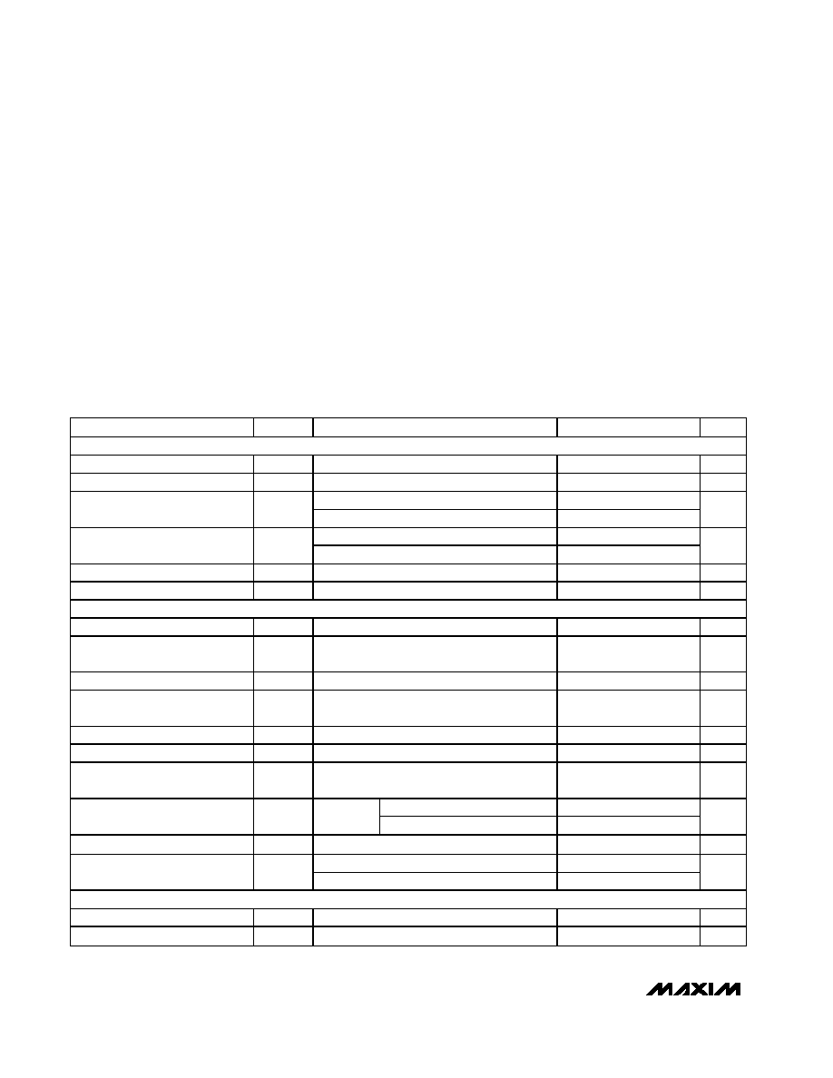
DC ELECTRICAL CHARACTERISTICS
(VCC = 3.0V to 3.6V, RL = 100 ±1%,
|VID| = 0.05V to 1.2V, VCM = |VID / 2| to 2.4V - |VID / 2|, TA = -40°C to +85°C, unless otherwise
noted. Typical values are at VCC = 3.3V, TA = +25°C.) (Notes 1, 2)
PARAMETER
SYMBOL
CONDITIONS
MIN
TYP
MAX
UNITS
LVDS INPUT
Differential Input High Threshold
VTH
750
mV
Differential Input Low Threshold
VTL
-50
-7
mV
0.05V
≤ |VID| ≤ 0.6V
-15
-2.5
+15
Input Current
IIN+, IIN-
0.6V <
|VID| ≤ 1.2V
-20
-3.5
+20
A
0.05V
≤ |VID| ≤ 0.6V, VCC = 0V
-15
+1.3
+15
Power-Off Input Current
IIN+, IIN-
0.6V <
|VID| ≤ 1.2V, VCC = 0V
-20
+2.6
+20
A
Input Resistor 1
RIN1
VCC = 3.6V or 0V, Figure 1
67
232
k
Input Resistor 2
RIN2
VCC = 3.6V or 0V, Figure 1
267
1174
k
LVDS OUTPUT
Differential Output Voltage
VOD
Figure 2
250
360
450
mV
Change in VOD Between
Complementary Output States
VOD
Figure 2
0.008
25
mV
Offset (Common-Mode) Voltage
VOS
Figure 2
1.125
1.25
1.375
V
Change in VOS for
Complementary Output States
VOS
Figure 2
0.005
25
mV
Output High Voltage
VOH
1.44
1.6
V
Output Low Voltage
VOL
0.9
1.08
V
Fail-Safe Differential Output
Voltage
VOD+
IN+, IN- shorted, open, or parallel
terminated
+250
+360
+450
mV
OUT+ = 3.6V, other output open
-10
+0.02
+10
Power-Off Output Leakage
Current
IOOFF
VCC = 0V
OUT- = 3.6V, other output open
-10
+0.02
+10
A
Differential Output Resistance
RODIFF
VCC = 3.6V or 0V
100
260
400
VID = 50mV, OUT+ = GND
-5
-15
Output Short Current
ISC
VID = -50mV, OUT- = GND
-5
-15
mA
POWER SUPPLY
Supply Current
ICC
Output loaded
10
15
mA
Supply Current in Fail-Safe
ICCF
Output loaded, input undriven
6
8
mA
相关PDF资料 |
PDF描述 |
|---|---|
| MAX9205EAI/V+T | IC SERIALIZER 10BIT LVDS 28SSOP |
| MAX9208EAI+ | IC DESERIALIZER LVDS 28-SSOP |
| MAX9209GUM+D | IC PROG DC-BAL 21BIT SER 48TSSOP |
| MAX9213EUM+ | IC SERIALIZER PROG 48-TSSOP |
| MAX9214EUM+TD | IC DESERIALIZER PROG 48TSSOP |
相关代理商/技术参数 |
参数描述 |
|---|---|
| MAX9181 | 制造商:MAXIM 制造商全称:Maxim Integrated Products 功能描述:Low-Jitter.Low-Noise LVPECL-to-LVDS Level Translator in an SC70 Package |
| MAX9181EXT | 制造商:Maxim Integrated Products 功能描述:LOW-JITTER, LOW-NOISE LVPECL-TO-LVDS LEVEL TR - Cut Tape Product |
| MAX9181EXT-T | 制造商:Maxim Integrated Products 功能描述:LOW-JITTER, LOW-NOISE LVPECL-TO-LVDS LEVEL TR - Tape and Reel |
| MAX918ESA | 功能描述:校验器 IC RoHS:否 制造商:STMicroelectronics 产品: 比较器类型: 通道数量: 输出类型:Push-Pull 电源电压-最大:5.5 V 电源电压-最小:1.1 V 补偿电压(最大值):6 mV 电源电流(最大值):1350 nA 响应时间: 最大工作温度:+ 125 C 安装风格:SMD/SMT 封装 / 箱体:SC-70-5 封装:Reel |
| MAX918ESA+ | 功能描述:校验器 IC 1.8V nPower Comparator RoHS:否 制造商:STMicroelectronics 产品: 比较器类型: 通道数量: 输出类型:Push-Pull 电源电压-最大:5.5 V 电源电压-最小:1.1 V 补偿电压(最大值):6 mV 电源电流(最大值):1350 nA 响应时间: 最大工作温度:+ 125 C 安装风格:SMD/SMT 封装 / 箱体:SC-70-5 封装:Reel |
发布紧急采购,3分钟左右您将得到回复。