- 您现在的位置:买卖IC网 > PDF目录11687 > MAX9242EUM/V+T (Maxim Integrated Products)IC DESERIALIZER 21BIT 48TSSOP PDF资料下载
参数资料
| 型号: | MAX9242EUM/V+T |
| 厂商: | Maxim Integrated Products |
| 文件页数: | 10/23页 |
| 文件大小: | 0K |
| 描述: | IC DESERIALIZER 21BIT 48TSSOP |
| 标准包装: | 2,500 |
| 系列: | * |
MAX9242/MAX9244/MAX9246/MAX9254
21-Bit Deserializers with Programmable
Spread Spectrum and DC Balance
18
______________________________________________________________________________________
The capacitor value decreases for a higher frequency
parallel clock and for higher levels of droop and jitter.
Use high-frequency, surface-mount ceramic capacitors.
Equation 1 altered for four series capacitors (Figure 20) is:
C = -(4 x tB x DSV) / (ln (1 - D) x (RT + RO)) (Eq 3)
Fail-Safe
The MAX9242/MAX9244/MAX9246/MAX9254 have fail-
safe LVDS inputs in non-DC-balanced mode (Figure 1).
Fail-safe drives the outputs low when the corresponding
LVDS input is open, undriven and shorted, or undriven
and parallel terminated. The fail-safe on the LVDS clock
input drives all outputs low when power is stable. Fail-
safe does not operate in DC-balanced mode.
Input Bias and Frequency Detection
In DC-balanced mode, the inverting and noninverting
LVDS inputs are internally connected to +1.2V through
42k
Ω (min) to provide biasing for AC-coupling (Figure 1).
To prevent switching due to noise when the clock input
is not driven, bias the clock inputs (RxCLKIN+,
RxCLKIN-) to differential +15mV by connecting a 10k
Ω
±1% pullup resistor between the noninverting input and
LVDSVCC, and a 10k
Ω ±1% pulldown resistor between
the inverting input and ground. These bias resistors,
along with the 100
Ω ±1% tolerant termination resistor,
provide +15mV of differential input. The +15mV bias
causes some small degradation of RSKM proportional to
the slew rate of the clock input. For example, if the clock
transitions 250mV in 500ps, the slew rate of 0.5mV/ps
reduces RSKM by 30ps.
Unused LVDS Data Inputs
In non-DC-balanced mode, leave unused LVDS data
inputs open. In non-DC-balanced mode, the input fail-
safe circuit drives the corresponding outputs low, and no
pullup or pulldown resistors are needed. In DC-balanced
mode, at each unused LVDS data input, pull the inverting
input up to LVDSVCC using a 10k
Ω resistor, and pull the
noninverting input down to ground using a 10k
Ω resistor.
Do not connect a termination resistor. The pullup and
pulldown resistors drive the corresponding outputs low
and prevent switching due to noise.
(7 + 2):1
7
100
Ω
(7 + 2):1
7
100
Ω
(7 + 2):1
1:(9 - 2)
+ FIFO
1:(9 - 2)
+ FIFO
1:(9 - 2)
+ FIFO
7
100
Ω
PLL
100
Ω
MAX9209/MAX9213
MAX9242/MAX9244/MAX9246/MAX9254
TxOUT
TxCLK OUT
RxIN__
RxCLK IN
21:3 SERIALIZER
3:21 DESERIALIZER
PWRDWN
RxCLK OUT
RxOUT_
PWRDWN
TxCLK IN
TxIN
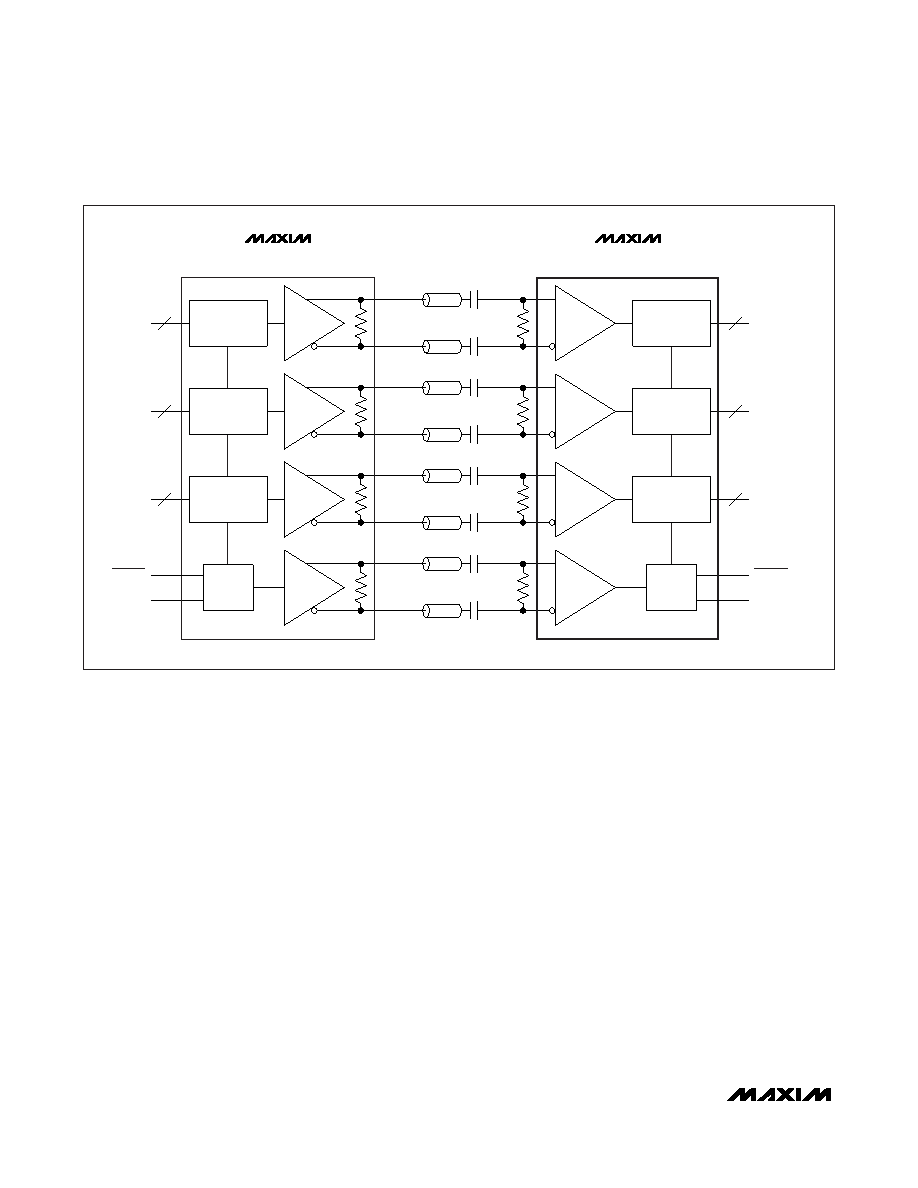
HIGH-FREQUENCY, CERAMIC
SURFACE-MOUNT CAPACITORS
CAN ALSO BE PLACED AT THE
SERIALIZER INSTEAD OF THE DESERIALIZER.
PLL1 +
SSPLL
RO
RT
Figure 19. Two Capacitors per Link, AC-Coupled, DC-Balanced Mode
相关PDF资料 |
PDF描述 |
|---|---|
| MAX9246EUM+TD | IC 21BIT DESERIALIZER 48-TSSOP |
| D38999/20WH55SB | CONN RCPT 55POS WALL MNT W/SCKT |
| MS27484T24A61SA | CONN PLUG 61POS STRAIGHT W/SCKT |
| R5F100PJAFB#V0 | MCU 16BIT 256KB FLASH 100LQFP |
| D38999/26JF11PA | CONN PLUG 11POS STRAIGHT W/PINS |
相关代理商/技术参数 |
参数描述 |
|---|---|
| MAX9242GUM | 制造商:MAXIM 制造商全称:Maxim Integrated Products 功能描述:21-Bit Deserializers with Programmable Spread Spectrum and DC Balance |
| MAX9242GUM/V+ | 功能描述:串行器/解串器 - Serdes 21-Bit DC-Balanced LVDS Deserializer RoHS:否 制造商:Texas Instruments 类型:Deserializer 数据速率:1.485 Gbit/s 输入类型:ECL/LVDS 输出类型:LVCMOS 输入端数量:1 输出端数量:20 工作电源电压:2.375 V to 2.625 V 工作温度范围:0 C to + 70 C 封装 / 箱体:TQFP-64 |
| MAX9242GUM/V+T | 功能描述:串行器/解串器 - Serdes 21-Bit DC-Balanced LVDS Deserializer RoHS:否 制造商:Texas Instruments 类型:Deserializer 数据速率:1.485 Gbit/s 输入类型:ECL/LVDS 输出类型:LVCMOS 输入端数量:1 输出端数量:20 工作电源电压:2.375 V to 2.625 V 工作温度范围:0 C to + 70 C 封装 / 箱体:TQFP-64 |
| MAX9242GUM+D | 功能描述:串行器/解串器 - Serdes 21-Bit DC-Balanced LVDS Deserializer RoHS:否 制造商:Texas Instruments 类型:Deserializer 数据速率:1.485 Gbit/s 输入类型:ECL/LVDS 输出类型:LVCMOS 输入端数量:1 输出端数量:20 工作电源电压:2.375 V to 2.625 V 工作温度范围:0 C to + 70 C 封装 / 箱体:TQFP-64 |
| MAX9242GUM+TD | 功能描述:串行器/解串器 - Serdes 21-Bit DC-Balanced LVDS Deserializer RoHS:否 制造商:Texas Instruments 类型:Deserializer 数据速率:1.485 Gbit/s 输入类型:ECL/LVDS 输出类型:LVCMOS 输入端数量:1 输出端数量:20 工作电源电压:2.375 V to 2.625 V 工作温度范围:0 C to + 70 C 封装 / 箱体:TQFP-64 |
发布紧急采购,3分钟左右您将得到回复。