- 您现在的位置:买卖IC网 > PDF目录8679 > MAX9310AEUP+ (Maxim Integrated Products)IC CLOCK DRVR 1.0GHZ 20TSSOP PDF资料下载
参数资料
| 型号: | MAX9310AEUP+ |
| 厂商: | Maxim Integrated Products |
| 文件页数: | 10/11页 |
| 文件大小: | 0K |
| 描述: | IC CLOCK DRVR 1.0GHZ 20TSSOP |
| 标准包装: | 74 |
| 类型: | 扇出缓冲器(分配),多路复用器 |
| 电路数: | 1 |
| 比率 - 输入:输出: | 2:5 |
| 差分 - 输入:输出: | 是/是 |
| 输入: | HSTL,LVPECL |
| 输出: | LVDS |
| 频率 - 最大: | 1GHz |
| 电源电压: | 3 V ~ 3.6 V |
| 工作温度: | -40°C ~ 85°C |
| 安装类型: | * |
| 封装/外壳: | * |
| 供应商设备封装: | * |
| 包装: | * |
MAX9310A
1:5 Clock Driver with Selectable LVPECL
Inputs/Single-Ended Inputs and LVDS Outputs
8
_______________________________________________________________________________________
Detailed Description
The MAX9310A is a low-skew 1:5 differential driver with
two selectable LVPECL inputs and LVDS outputs,
designed for clock distribution applications. The select-
ed clock accepts a differential input signal and repro-
duces it on five separate differential LVDS outputs. The
inputs are biased with internal resistors such that the
output is differential low when inputs are open. An on-
chip VBB reference output is available for single-ended
input operation. The device is guaranteed to operate at
frequencies up to 1.0GHz with LVDS output levels con-
forming to the EIA/TIA-644 standard.
The MAX9310A is designed for 3V to 3.6V operation in
systems with a nominal 3.3V supply.
Differential LVPECL Input
The MAX9310A has two input differential pairs that
accept differential LVPECL/HSTL inputs, and can be
configured to accept single-ended LVPECL inputs
through the use of the VBB voltage-reference output.
Each differential input pair has to be independently ter-
minated. A select pin (CLKSEL) is used to activate the
desired input. The maximum magnitude of the differen-
tial signal applied to the input is 3V. Specifications for
the high and low voltages of a differential input (VIHD
and VILD) and the differential input voltage (VIHD - VILD)
apply simultaneously.
Single-Ended Inputs and VBB
The differential inputs can be configured to accept a
single-ended input through the use of the VBB refer-
ence voltage. A noninverting, single-ended input is pro-
duced by connecting VBB to the CLK_ input and
applying a single-ended signal to the CLK_ input.
Similarly, an inverting input is produced by connecting
VBB to the CLK_ input and applying the signal to the
CLK_ input. With a differential input configured as sin-
gle ended (using VBB), the single-ended input can be
driven to VCC and GND, or with a single-ended
LVPECL signal. Note the single-ended input must be at
least VBB ±95mV or a differential input of at least 95mV
to switch the outputs to the VOH and VOL levels speci-
fied in the DC Electrical Characteristics table (Figure 1).
When using the VBB reference output, bypass it with a
0.01F ceramic capacitor to VCC. If the VBB reference
is not used, leave unconnected. The VBB reference can
source or sink 500A. Use VBB only for inputs that are
on the same device as the VBB reference.
Synchronous Enable
The MAX9310A is synchronously enabled and disabled
with outputs in a differential low state to eliminate short-
ened clock pulses. EN is connected to the input of an
edge-triggered D flip-flop. After power-up, drive EN low
and toggle the selected clock input to enable the out-
puts. The outputs are enabled on the falling edge of the
selected clock input after EN goes low. The outputs are
set to a differential low state on the falling edge of the
selected clock input after EN goes high (Figure 3).
Input Bias Resistors
Internal biasing resistors ensure a (differential) output
low condition in the event that the inputs are not con-
nected. The inverting input (CLK_) is biased with a
75k
pulldown to GND and a 75k pullup to VCC. The
noninverting input (CLK_) is biased with a 75k
pull-
down to GND.
Differential LVDS Output
The LVDS outputs must be terminated with 100
across Q and Q, as shown in the Typical Application
Circuit. The outputs are short-circuit protected.
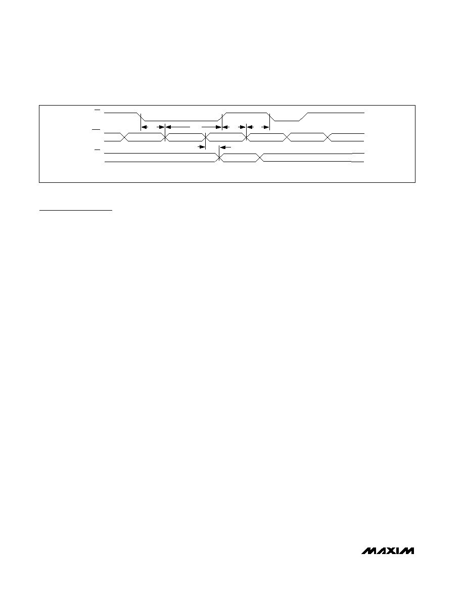
tS
tH
tS
tPLHD
OUTPUTS ARE LOW
OUTPUTS STAY LOW
EN
CLK
Q_
tH
tS = SETUP TIME
tH = HOLD TIME
Figure 3. MAX9310A Timing EN Diagram
相关PDF资料 |
PDF描述 |
|---|---|
| AD7305BRU-REEL7 | IC DAC 8BIT QUAD R-R 20-TSSOP |
| VE-J5W-MY | CONVERTER MOD DC/DC 5.5V 50W |
| VI-J1P-MX-B1 | CONVERTER MOD DC/DC 13.8V 75W |
| V300A24H500B3 | CONVERTER MOD DC/DC 24V 500W |
| MAX9325EQI+ | IC CLK/DATA BUFF MUX 2:8 28-PLCC |
相关代理商/技术参数 |
参数描述 |
|---|---|
| MAX9310AEUP+ | 功能描述:时钟驱动器及分配 1:5 Clock Driver RoHS:否 制造商:Micrel 乘法/除法因子:1:4 输出类型:Differential 最大输出频率:4.2 GHz 电源电压-最大: 电源电压-最小:5 V 最大工作温度:+ 85 C 封装 / 箱体:SOIC-8 封装:Reel |
| MAX9310AEUP+T | 功能描述:时钟驱动器及分配 1:5 Clock Driver RoHS:否 制造商:Micrel 乘法/除法因子:1:4 输出类型:Differential 最大输出频率:4.2 GHz 电源电压-最大: 电源电压-最小:5 V 最大工作温度:+ 85 C 封装 / 箱体:SOIC-8 封装:Reel |
| MAX9310AEUP-T | 制造商:Maxim Integrated Products 功能描述:1:5 CLOCK DRIVER WITH SELECTABLE LVPECL INPUT - Tape and Reel |
| MAX9310EUP | 制造商:Maxim Integrated Products 功能描述:1:5 CLOCK DRIVER WITH SELECTABLE LVPECL INPUT - Bulk |
| MAX9310EUP+ | 制造商:Maxim Integrated Products 功能描述:CLOCK DRVR 2-IN LVDS 20TSSOP - Rail/Tube |
发布紧急采购,3分钟左右您将得到回复。