- 您现在的位置:买卖IC网 > PDF目录2089 > MAX9310AEUP+T (Maxim Integrated Products)IC CLOCK DRVR 1.0GHZ 20TSSOP PDF资料下载
参数资料
| 型号: | MAX9310AEUP+T |
| 厂商: | Maxim Integrated Products |
| 文件页数: | 6/11页 |
| 文件大小: | 0K |
| 描述: | IC CLOCK DRVR 1.0GHZ 20TSSOP |
| 标准包装: | 2,500 |
| 类型: | 扇出缓冲器(分配),多路复用器 |
| 电路数: | 1 |
| 比率 - 输入:输出: | 2:5 |
| 差分 - 输入:输出: | 是/是 |
| 输入: | HSTL,LVPECL |
| 输出: | LVDS |
| 频率 - 最大: | 1GHz |
| 电源电压: | 3 V ~ 3.6 V |
| 工作温度: | -40°C ~ 85°C |
| 安装类型: | * |
| 封装/外壳: | * |
| 供应商设备封装: | * |
| 包装: | * |
MAX9310A
4
_______________________________________________________________________________________
Note 1: Measurements are made with the device in thermal equilibrium.
Note 2: Current into a pin is defined as positive. Current out of a pin is defined as negative.
Note 3: DC parameters are production tested at +25°C. DC limits are guaranteed by design and
characterized over the full operating temperature range.
Note 4: Use VBB only for inputs that are on the same device as the VBB reference.
Note 5: All pins are open except VCC and GND, all outputs are loaded with 100
differentially.
Note 6: Guaranteed by design and characterization. Limits are set to ±6 sigma.
Note 7: Measured between outputs of the same part at the signal crossing points for a same-edge
transition.
Note 8: Measured between outputs of different parts at the signal crossing points under identical conditions
for a same-edge transition.
Note 9: Device jitter added to the input signal.
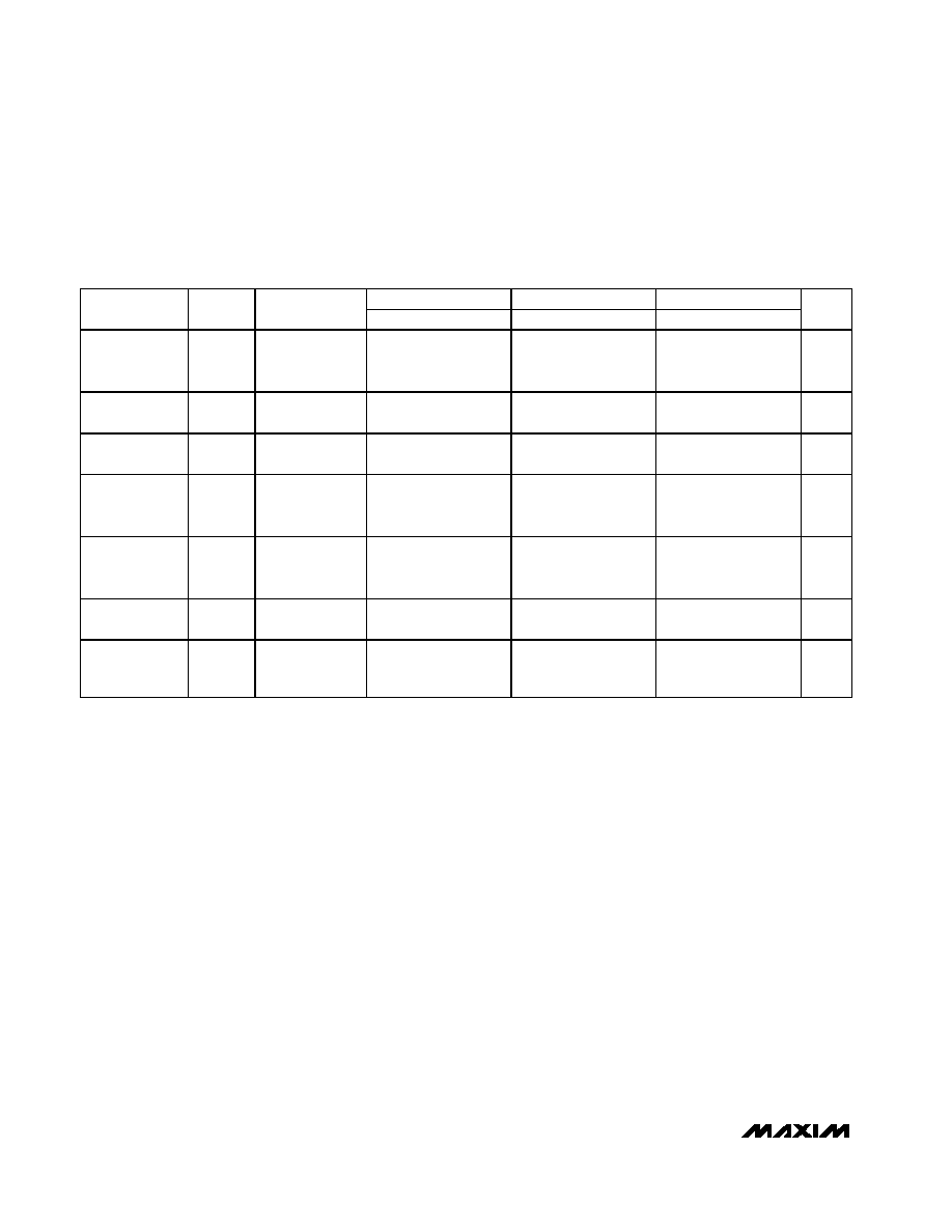
AC ELECTRICAL CHARACTERISTICS
(VCC - GND = 3V to 3.6V, outputs terminated with 100
±1%, fIN ≤ 1.0GHz, input transition time = 125ps (20% to 80%),
VIHD - VILD = 0.15V to VCC, unless otherwise noted. Typical values are at VCC - GND = 3.3V, VIHD = VCC - 1.0V, VILD = VCC - 1.5V,
unless otherwise noted.) (Notes 1 and 6)
-40
°C
+25
°C
+85
°C
PARAMETER
SYMBOL
CONDITIONS
MIN
TYP
MAX
MIN
TYP
MAX
MIN
TYP
MAX
UNITS
Propagation
Delay CLK_,
CLK_ to Q_, Q_
tPHL,
tPLH
Figure 2
250
340
600
250
340
600
250
340
600
ps
Output-to-
Output Skew
tSKOO
(Note 7)
10
30
8
25
20
45
ps
Part-to-Part
Skew
tSKPP
(Note 8)
145
ps
Added Random
Jitter
tRJ
fIN = 1.0GHz,
clock pattern
(Note 9)
0.3
1.0
0.3
1.0
0.3
1.0
ps
(RMS)
Added
Deterministic
Jitter
tDJ
fIN = 1.0Gsps,
2
23 - 1 PRBS
pattern (Note 9)
50
60
50
60
50
60
ps
(P-P)
Operating
Frequency
fMAX
VOD
≥ 250mV
1.0
GHz
Differential
Output Rise/Fall
Time
tR/tF
20% to 80%,
Figure 2
140
205
300
140
205
300
140
205
300
ps
1:5 Clock Driver with Selectable LVPECL
Inputs/Single-Ended Inputs and LVDS Outputs
相关PDF资料 |
PDF描述 |
|---|---|
| MAX9311ECJ+T | IC CLK/DATA BUFF MUX 2:10 32LQFP |
| MAX9312ECJ+T | IC CLK/DATA BUFF 1:5 3GHZ 32LQFP |
| MAX9315EUP+T | IC CLK/DATA BUFF MUX 2:5 20TSSOP |
| MAX9316EWP+T | IC CLOCK BUFFER MUX 2:5 20-SOIC |
| MAX9320ESA+T | IC CLOCK BUFFER 2:2 3GHZ 8-SOIC |
相关代理商/技术参数 |
参数描述 |
|---|---|
| MAX9310EUP | 制造商:Maxim Integrated Products 功能描述:1:5 CLOCK DRIVER WITH SELECTABLE LVPECL INPUT - Bulk |
| MAX9310EUP+ | 制造商:Maxim Integrated Products 功能描述:CLOCK DRVR 2-IN LVDS 20TSSOP - Rail/Tube |
| MAX9310EUP+T | 制造商:Maxim Integrated Products 功能描述:CLOCK DRVR 2-IN LVDS 20TSSOP - Tape and Reel |
| MAX9310EUP-T | 制造商:Maxim Integrated Products 功能描述:1:5 CLOCK DRIVER WITH SELECTABLE LVPECL INPUT - Tape and Reel |
| MAX9311ECJ | 功能描述:时钟缓冲器 RoHS:否 制造商:Texas Instruments 输出端数量:5 最大输入频率:40 MHz 传播延迟(最大值): 电源电压-最大:3.45 V 电源电压-最小:2.375 V 最大功率耗散: 最大工作温度:+ 85 C 最小工作温度:- 40 C 封装 / 箱体:LLP-24 封装:Reel |
发布紧急采购,3分钟左右您将得到回复。