- 您现在的位置:买卖IC网 > PDF目录8679 > MAX9315EUP+ (Maxim Integrated Products)IC CLK/DATA BUFF MUX 2:5 20TSSOP PDF资料下载
参数资料
| 型号: | MAX9315EUP+ |
| 厂商: | Maxim Integrated Products |
| 文件页数: | 6/11页 |
| 文件大小: | 0K |
| 描述: | IC CLK/DATA BUFF MUX 2:5 20TSSOP |
| 产品培训模块: | Lead (SnPb) Finish for COTS Obsolescence Mitigation Program |
| 标准包装: | 74 |
| 类型: | 扇出缓冲器(分配),多路复用器,数据 |
| 电路数: | 1 |
| 比率 - 输入:输出: | 2:5 |
| 差分 - 输入:输出: | 是/是 |
| 输入: | HSTL,LVECL,LVPECL |
| 输出: | LVECL,LVPECL |
| 频率 - 最大: | 1.5GHz |
| 电源电压: | 2.25 V ~ 3.8 V |
| 工作温度: | -40°C ~ 85°C |
| 安装类型: | 表面贴装 |
| 封装/外壳: | 20-TSSOP(0.173",4.40mm 宽) |
| 供应商设备封装: | 20-TSSOP |
| 包装: | 管件 |
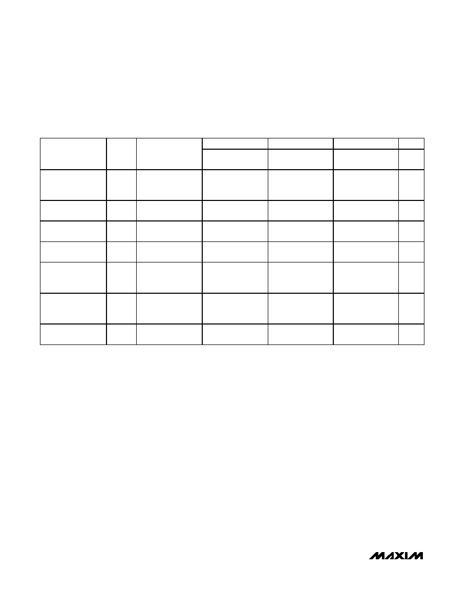
MAX9315
1:5 Differential LVPECL/LVECL/HSTL
Clock and Data Driver
4
_______________________________________________________________________________________
AC ELECTRICAL CHARACTERISTICS
(VCC - VEE = 2.375V to 3.8V, outputs loaded with 50
±1% to VCC - 2V, input frequency = 1.5GHz, input transition time = 125ps (20%
to 80%), SEL = high or low, EN = low, VIHD = VEE + 1.2V to VCC, VILD = VEE to VCC - 0.15V, VIHD - VILD = 0.15V to the smaller of 3V or
VCC - VEE, unless otherwise noted. Typical values are at VCC - VEE = +3.3V, VIHD = VCC - 1V, VILD = VCC - 1.5V.) (Notes 1, 7)
-40
°C
+25
°C
+85
°C
UNITS
PARAMETER
SYMBOL
CONDITIONS
MIN
TYP
MAX
MIN
TYP
MAX
MIN
TYP
MAX
ps
Differential Input-
to-Output Delay
tPLHD,
tPHLD
Figure 2
290
400
310
440
300
520
ps
Output-to-Output
Skew (Note 8)
tSKOO
5
30
20
40
20
50
ps
Part-to-Part Skew
(Note 9)
tSKPP
110
130
220
ps
Added Random
Jitter (Note 10)
tRJ
fIN = 1.5GHz clock
0.8
1.2
0.8
1.2
0.8
1.2
ps (RMS)
Added
Deterministic Jitter
(Note 10)
tDJ
1.5Gbps 2E23-1
PRBS pattern
50
70
50
70
50
70
ps (p-p)
Switching
Frequency
fMAX
(VOH - VOL)
≥
400mV,
Figure 2
1.5
GHz
Output Rise/Fall
Time (20% to 80%)
tR, tF
Figure 2
80
120
90
130
90
145
ps
Note 1: Measurements are made with the device in thermal equilibrium.
Note 2: Current into a pin is defined as positive. Current out of a pin is defined as negative.
Note 3: DC parameters production tested at TA = +25°C and guaranteed by design over the full operating temperature range.
Note 4: Single-ended input operation using VBB is limited to VCC - VEE = 3.0V to 3.8V.
Note 5: Use VBB only for inputs that are on the same device as the VBB reference.
Note 6: All pins open except VCC and VEE.
Note 7: Guaranteed by design and characterization. Limits are set at ±6 sigma.
Note 8: Measured between outputs of the same part at the signal crossing points for a same-edge transition.
Note 9: Measured between outputs of different parts at the signal crossing points under identical conditions for a same-edge transition.
Note 10: Device jitter added to the input signal.
相关PDF资料 |
PDF描述 |
|---|---|
| VE-J5Y-MW | CONVERTER MOD DC/DC 3.3V 66W |
| V300A15H500BF2 | CONVERTER MOD DC/DC 15V 500W |
| MAX9312ETJ+ | IC CLK/DATA BUFF 1:5 3GHZ 32TQFN |
| V300A15H500BF | CONVERTER MOD DC/DC 15V 500W |
| V300A15H500BL2 | CONVERTER MOD DC/DC 15V 500W |
相关代理商/技术参数 |
参数描述 |
|---|---|
| MAX9315EUP+ | 功能描述:时钟驱动器及分配 LVPECL/LVECL/HSTL Clock & Data Driver RoHS:否 制造商:Micrel 乘法/除法因子:1:4 输出类型:Differential 最大输出频率:4.2 GHz 电源电压-最大: 电源电压-最小:5 V 最大工作温度:+ 85 C 封装 / 箱体:SOIC-8 封装:Reel |
| MAX9315EUP+T | 功能描述:时钟驱动器及分配 LVPECL/LVECL/HSTL Clock & Data Driver RoHS:否 制造商:Micrel 乘法/除法因子:1:4 输出类型:Differential 最大输出频率:4.2 GHz 电源电压-最大: 电源电压-最小:5 V 最大工作温度:+ 85 C 封装 / 箱体:SOIC-8 封装:Reel |
| MAX9315EUP-T | 功能描述:时钟驱动器及分配 RoHS:否 制造商:Micrel 乘法/除法因子:1:4 输出类型:Differential 最大输出频率:4.2 GHz 电源电压-最大: 电源电压-最小:5 V 最大工作温度:+ 85 C 封装 / 箱体:SOIC-8 封装:Reel |
| MAX9315EUP-TG068 | 制造商:Maxim Integrated Products 功能描述:1:5 DIFFERENTIAL LVPECL/LVECL/HSTL CLOCK AND - Rail/Tube |
| MAX9315EVKIT | 功能描述:时钟驱动器及分配 Evaluation Kit for the MAX9315 MAX9316 RoHS:否 制造商:Micrel 乘法/除法因子:1:4 输出类型:Differential 最大输出频率:4.2 GHz 电源电压-最大: 电源电压-最小:5 V 最大工作温度:+ 85 C 封装 / 箱体:SOIC-8 封装:Reel |
发布紧急采购,3分钟左右您将得到回复。