- 您现在的位置:买卖IC网 > PDF目录26790 > MAX9320XESA (MAXIM INTEGRATED PRODUCTS INC) 9320 SERIES, LOW SKEW CLOCK DRIVER, 2 TRUE OUTPUT(S), 0 INVERTED OUTPUT(S), PDSO8 PDF资料下载
参数资料
| 型号: | MAX9320XESA |
| 厂商: | MAXIM INTEGRATED PRODUCTS INC |
| 元件分类: | 时钟及定时 |
| 英文描述: | 9320 SERIES, LOW SKEW CLOCK DRIVER, 2 TRUE OUTPUT(S), 0 INVERTED OUTPUT(S), PDSO8 |
| 封装: | 0.150 INCH, MS-012, SOIC-8 |
| 文件页数: | 8/10页 |
| 文件大小: | 614K |
| 代理商: | MAX9320XESA |
MAX9320/MAX9320A
1:2 Differential LVPECL/LVECL/HSTL
Clock and Data Drivers
_______________________________________________________________________________________
7
Detailed Description
The MAX9320/MAX9320A low-skew, 1-to-2 differential
drivers are designed for clock and data distribution. For
interfacing to differential HSTL and LVPECL signals,
these devices operate over a +2.25V to +3.8V supply
range, allowing high-performance clock and data distri-
bution in systems with a nominal +2.5V or +3.3V sup-
ply. For differential LVECL operation, these devices
operate from a -2.25V to -3.8V supply.
Inputs
The maximum magnitude of the differential input from D
to
D is VCC - VEE or 3.0V, whichever is less. This limit
also applies to the difference between any reference
voltage input and a single-ended input.
The differential inputs have bias resistors that drive the
outputs to a differential low when the inputs are open.
The inverting input,
D, is biased with a 60k pullup to
VCC and a 100k pulldown to VEE. The noninverting
input, D, is biased with a 100k pulldown to VEE.
Specifications for the high and low voltages of the dif-
ferential input (VIHD and VILD) and the differential input
voltage (VIHD - VILD) apply simultaneously (VILD cannot
be higher than VIHD).
Outputs
Output levels are referenced to VCC and are consid-
ered LVPECL or LVECL, depending on the level of the
VCC supply. With VCC connected to a positive supply
and VEE connected to GND, the outputs are LVPECL.
The outputs are LVECL when VCC is connected to GND
and VEE is connected to a negative supply.
A single-ended input of ±100mV around a reference
voltage or a differential input of at least ±100mV switch-
es the outputs to the VOH and VOL levels specified in
the DC Electrical Characteristics table.
Applications Information
Supply Bypassing
Bypass VCC to VEE with high-frequency surface-mount
ceramic 0.1F and 0.01F capacitors in parallel as
close to the device as possible, with the 0.01F value
capacitor closest to the device. Use multiple parallel
vias for low inductance.
Traces
Input and output trace characteristics affect the perfor-
mance of the MAX9320/MAX9320A. Connect each
signal of a differential input or output to a 50 charac-
teristic impedance trace. Minimize the number of vias
to prevent impedance discontinuities. Reduce reflec-
tions by maintaining the 50 characteristic impedance
through connectors and across cables. Reduce skew
within a differential pair by matching the electrical
length of the traces.
The exposed-pad (EP) SO package can be soldered to
the PC board for enhanced thermal performance. If the
EP is not soldered to the PC board, the thermal resis-
tance is the same as the regular SO package. The EP
is connected to the chip VEE supply. Be sure that the
pad does not touch signal lines or other supplies.
Contact the Maxim Packaging department for guide-
lines on the use of EP packages.
Output Termination
Terminate outputs through 50 to VCC - 2V or use an
equivalent Thevenin termination. Terminate both out-
puts and use the same termination on each for the low-
est output-to-output skew. When a single-ended signal
is taken from a differential output, terminate both out-
puts. For example, if Q0 is used as a single-ended out-
put, terminate both Q0 and
Q0.
Chip Information
TRANSISTOR COUNT: 182
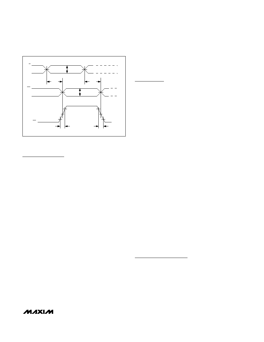
Figure 1. Differential Transition Time and Propagation Delay
Timing Diagram
0 (DIFFERENTIAL)
80%
20%
80%
20%
0 (DIFFERENTIAL)
VOH -VOL
VIHD -VILD
VIHD
VILD
VOH
VOL
Q_
Q
tPLHD
tPHLD
tR
tF
D
(Q_) - (Q_)
相关PDF资料 |
PDF描述 |
|---|---|
| MAX9325EGI | 9325 SERIES, LOW SKEW CLOCK DRIVER, 8 TRUE OUTPUT(S), 0 INVERTED OUTPUT(S), QCC28 |
| MAX9325ETI | LOW SKEW CLOCK DRIVER, 8 TRUE OUTPUT(S), 0 INVERTED OUTPUT(S), QCC28 |
| MB2053B | MB SERIES, DUAL 8-BIT REGISTERED TRANSCEIVER, INVERTED OUTPUT, PQFP52 |
| MB2240B | MB SERIES, QUAD 4-BIT DRIVER, INVERTED OUTPUT, PQFP52 |
| MB2241B | MB SERIES, QUAD 4-BIT DRIVER, TRUE OUTPUT, PQFP52 |
相关代理商/技术参数 |
参数描述 |
|---|---|
| MAX9321AEKA | 制造商:Maxim Integrated Products 功能描述:DIFFERENTIAL LVPECL/LVECL/HSTL RECEIVER/DRIVE - Rail/Tube |
| MAX9321AEKA-T | 制造商:Maxim Integrated Products 功能描述:DIFFERENTIAL LVPECL/LVECL/HSTL RECEIVER/DRIVE - Tape and Reel |
| MAX9321AESA | 功能描述:总线收发器 LVPECL/LVECL/HSTL Receiver/Driver RoHS:否 制造商:Fairchild Semiconductor 逻辑类型:CMOS 逻辑系列:74VCX 每芯片的通道数量:16 输入电平:CMOS 输出电平:CMOS 输出类型:3-State 高电平输出电流:- 24 mA 低电平输出电流:24 mA 传播延迟时间:6.2 ns 电源电压-最大:2.7 V, 3.6 V 电源电压-最小:1.65 V, 2.3 V 最大工作温度:+ 85 C 封装 / 箱体:TSSOP-48 封装:Reel |
| MAX9321AESA+ | 功能描述:总线收发器 RoHS:否 制造商:Fairchild Semiconductor 逻辑类型:CMOS 逻辑系列:74VCX 每芯片的通道数量:16 输入电平:CMOS 输出电平:CMOS 输出类型:3-State 高电平输出电流:- 24 mA 低电平输出电流:24 mA 传播延迟时间:6.2 ns 电源电压-最大:2.7 V, 3.6 V 电源电压-最小:1.65 V, 2.3 V 最大工作温度:+ 85 C 封装 / 箱体:TSSOP-48 封装:Reel |
| MAX9321AESA+T | 功能描述:时钟驱动器及分配 RoHS:否 制造商:Micrel 乘法/除法因子:1:4 输出类型:Differential 最大输出频率:4.2 GHz 电源电压-最大: 电源电压-最小:5 V 最大工作温度:+ 85 C 封装 / 箱体:SOIC-8 封装:Reel |
发布紧急采购,3分钟左右您将得到回复。