- 您现在的位置:买卖IC网 > PDF目录10652 > MAX942AUA+ (Maxim Integrated Products)IC COMPARATOR R-R 8-UMAX PDF资料下载
参数资料
| 型号: | MAX942AUA+ |
| 厂商: | Maxim Integrated Products |
| 文件页数: | 12/14页 |
| 文件大小: | 0K |
| 描述: | IC COMPARATOR R-R 8-UMAX |
| 产品培训模块: | Lead (SnPb) Finish for COTS Obsolescence Mitigation Program |
| 标准包装: | 50 |
| 类型: | 通用 |
| 元件数: | 2 |
| 输出类型: | CMOS,推挽式,TTL |
| 电压 - 电源,单路/双路(±): | 2.7 V ~ 5.5 V |
| 电压 - 输入偏移(最小值): | 3mV @ 5.5V |
| 电流 - 输入偏压(最小值): | 0.15µA @ 5.5V |
| 电流 - 静态(最大值): | 600µA |
| CMRR, PSRR(标准): | 81.94dB CMRR,81.94dB PSRR |
| 传输延迟(最大): | 80ns |
| 工作温度: | -40°C ~ 125°C |
| 封装/外壳: | 8-TSSOP,8-MSOP(0.118",3.00mm 宽) |
| 安装类型: | 表面贴装 |
| 包装: | 管件 |
_______________Detailed Description
The MAX941/MAX942/MAX944 single-supply compara-
tors feature internal hysteresis, high speed, and low
power. Their outputs are guaranteed to pull within 0.4V
of either supply rail without external pullup or pulldown
circuitry. Rail-to-rail input voltage range and low-volt-
age single-supply operation make these devices ideal
for portable equipment. The MAX941/MAX942/
MAX944 interface directly to CMOS and TTL logic.
Timing
Most high-speed comparators oscillate in the linear
region because of noise or undesired parasitic feed-
back. This tends to occur when the voltage on one
input is at or equal to the voltage on the other input. To
counter the parasitic effects and noise, the MAX941/
MAX942/MAX944 have internal hysteresis.
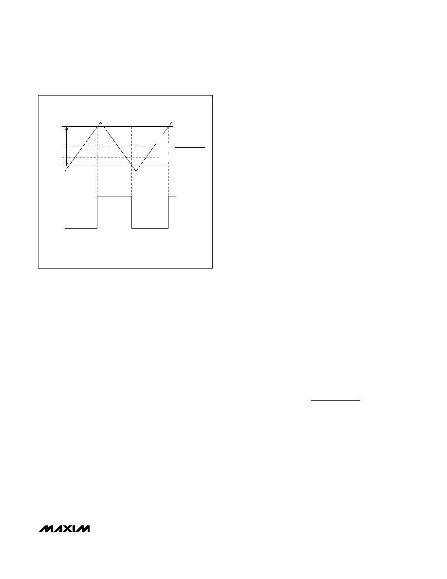
The hysteresis in a comparator creates two trip points:
one for the rising input voltage and one for the falling
input voltage (Figure 1). The difference between the trip
points is the hysteresis. When the comparator’s input
voltages are equal, the hysteresis effectively causes
one comparator input voltage to move quickly past the
other, thus taking the input out of the region where
oscillation occurs. Standard comparators require hys-
teresis to be added with external resistors. The
MAX941/MAX942/MAX944’s fixed internal hysteresis
eliminates these resistors and the equations needed to
determine appropriate values.
Figure 1 illustrates the case where IN- is fixed and IN+
is varied. If the inputs were reversed, the figure would
look the same, except the output would be inverted.
The MAX941 includes an internal latch that allows stor-
age of comparison results. The L
—
A
—
T
—
C
—
H
–
pin has a high
input impedance. If L
—
A
—
T
—
C
—
H
–
is high, the latch is transpar-
ent (i.e., the comparator operates as though the latch is
not present). The comparator's output state is stored
when L
—
A
—
T
—
C
—
H
–
is pulled low. All timing constraints must
be met when using the latch function (Figure 2).
Shutdown Mode (MAX941 Only)
The MAX941 shuts down when
–
S
—
H
—
D
—
N
–
is low. When shut
down, the supply current drops to less than 60A, and
the three-state output becomes high impedance. The
–
S
—
H
—
D
—
N
–
pin has a high input impedance. Connect
–
S
—
H
—
D
—
N
–
to V+ for normal operation. Exit shutdown with
L
—
A
—
T
—
C
—
H
–
high; otherwise, the output will be indeterminate.
Input Stage Circuitry
The MAX941/MAX942/MAX944 include internal protec-
tion circuitry that prevents damage to the precision
input stage from large differential input voltages. This
protection circuitry consists of two back-to-back diodes
between IN+ and IN- as well as two 4.1k resistors
(Figure 3). The diodes limit the differential voltage
applied to the internal circuitry of the comparators to be
no more than 2VF, where VF is the forward voltage drop
of the diode (about 0.7V at +25°C).
For a large differential input voltage (exceeding 2VF),
this protection circuitry increases the input bias current
at IN+ (source) and IN- (sink).
Input Current =
(IN+ - IN-) - 2VF
2 x 4.1k
Input current with large differential input voltages
should not be confused with input bias current (IB). As
long as the differential input voltage is less than 2VF,
this input current is equal to IB. The protection circuitry
also allows for the input common-mode range of the
MAX941/MAX942/MAX944 to extend beyond both
power-supply rails. The output is in the correct logic
state if one or both inputs are within the common-mode
range.
MAX941/MAX942/MAX944
High-Speed, Low-Power, 3V/5V, Rail-to-Rail,
Single-Supply Comparators
_______________________________________________________________________________________
7
VTRIP+
VHYST
VTRIP-
COMPARATOR
OUTPUT
VOH
VOL
VTRIP+ + VTRIP-
2
VOS =
VIN- = 0V
VIN+
Figure 1. Input and Output Waveform, Noninverting Input
Varied
相关PDF资料 |
PDF描述 |
|---|---|
| VI-B1M-IV-F1 | CONVERTER MOD DC/DC 10V 150W |
| MAX907CPA | IC COMPARATOR TTL DUAL HS 8-DIP |
| MAX488CPA+ | IC TXRX RS485/RS422 LOWPWR 8-DIP |
| MAX9042AESA+ | IC COMPARATOR DUAL 8-SOIC |
| VI-B1M-IV-F4 | CONVERTER MOD DC/DC 10V 150W |
相关代理商/技术参数 |
参数描述 |
|---|---|
| MAX942AUA+ | 功能描述:校验器 IC 3V/5V Rail-Rail Comparator RoHS:否 制造商:STMicroelectronics 产品: 比较器类型: 通道数量: 输出类型:Push-Pull 电源电压-最大:5.5 V 电源电压-最小:1.1 V 补偿电压(最大值):6 mV 电源电流(最大值):1350 nA 响应时间: 最大工作温度:+ 125 C 安装风格:SMD/SMT 封装 / 箱体:SC-70-5 封装:Reel |
| MAX942AUA+T | 功能描述:校验器 IC 3V/5V Rail-Rail Comparator RoHS:否 制造商:STMicroelectronics 产品: 比较器类型: 通道数量: 输出类型:Push-Pull 电源电压-最大:5.5 V 电源电压-最小:1.1 V 补偿电压(最大值):6 mV 电源电流(最大值):1350 nA 响应时间: 最大工作温度:+ 125 C 安装风格:SMD/SMT 封装 / 箱体:SC-70-5 封装:Reel |
| MAX942AUA-T | 功能描述:校验器 IC RoHS:否 制造商:STMicroelectronics 产品: 比较器类型: 通道数量: 输出类型:Push-Pull 电源电压-最大:5.5 V 电源电压-最小:1.1 V 补偿电压(最大值):6 mV 电源电流(最大值):1350 nA 响应时间: 最大工作温度:+ 125 C 安装风格:SMD/SMT 封装 / 箱体:SC-70-5 封装:Reel |
| MAX942C/D | 功能描述:校验器 IC RoHS:否 制造商:STMicroelectronics 产品: 比较器类型: 通道数量: 输出类型:Push-Pull 电源电压-最大:5.5 V 电源电压-最小:1.1 V 补偿电压(最大值):6 mV 电源电流(最大值):1350 nA 响应时间: 最大工作温度:+ 125 C 安装风格:SMD/SMT 封装 / 箱体:SC-70-5 封装:Reel |
| MAX942CPA | 功能描述:校验器 IC RoHS:否 制造商:STMicroelectronics 产品: 比较器类型: 通道数量: 输出类型:Push-Pull 电源电压-最大:5.5 V 电源电压-最小:1.1 V 补偿电压(最大值):6 mV 电源电流(最大值):1350 nA 响应时间: 最大工作温度:+ 125 C 安装风格:SMD/SMT 封装 / 箱体:SC-70-5 封装:Reel |
发布紧急采购,3分钟左右您将得到回复。