- 您现在的位置:买卖IC网 > PDF目录2090 > MAX9507ATE+T (Maxim Integrated Products)IC DIRECTDRIVE FILTER AMP 16TQFN PDF资料下载
参数资料
| 型号: | MAX9507ATE+T |
| 厂商: | Maxim Integrated Products |
| 文件页数: | 12/29页 |
| 文件大小: | 0K |
| 描述: | IC DIRECTDRIVE FILTER AMP 16TQFN |
| 产品培训模块: | Lead (SnPb) Finish for COTS Obsolescence Mitigation Program |
| 标准包装: | 2,500 |
| 系列: | DirectDrive® |
| 应用: | 滤波器 |
| 电路数: | 1 |
| -3db带宽: | 40.7MHz |
| 转换速率: | 35 V/µs |
| 电流 - 电源: | 3.1mA |
| 电流 - 输出 / 通道: | 82mA |
| 电压 - 电源,单路/双路(±): | 1.7 V ~ 2.63 V |
| 安装类型: | 表面贴装 |
| 封装/外壳: | 16-WFQFN 裸露焊盘 |
| 供应商设备封装: | 16-TQFN-EP(3x3) |
| 包装: | 带卷 (TR) |
| 配用: | MAX9507EVKIT+-ND - KIT EVAL FOR MAX9508 MAX9507EVCMAXQU+-ND - SYSTEM EVAL FOR MAX9507 KIT+MOD |
第1页第2页第3页第4页第5页第6页第7页第8页第9页第10页第11页当前第12页第13页第14页第15页第16页第17页第18页第19页第20页第21页第22页第23页第24页第25页第26页第27页第28页第29页
MAX9507
1.8V DirectDrive Video Filter Amplifier with
Load Detection and Dual SPST Analog Switches
2
_______________________________________________________________________________________
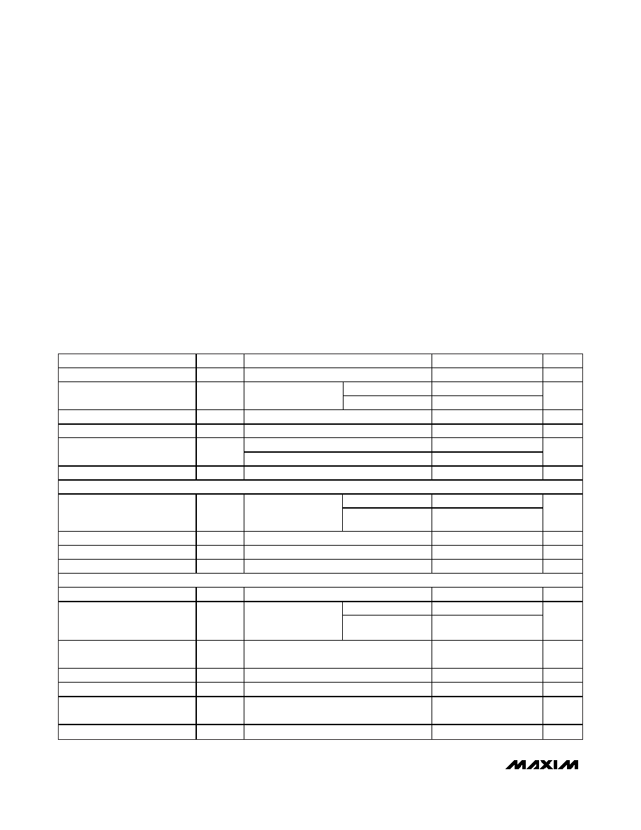
ABSOLUTE MAXIMUM RATINGS
ELECTRICAL CHARACTERISTICS
(VDD = +1.8V, GND = 0V, OUT has RL = 150Ω connected to GND, transparent sync-tip clamp enabled, C1 = C2 = 1F, TA = TMIN to
TMAX, unless otherwise noted. Typical values are at TA = +25°C.) (Note 1)
Stresses beyond those listed under “Absolute Maximum Ratings” may cause permanent damage to the device. These are stress ratings only, and functional
operation of the device at these or any other conditions beyond those indicated in the operational sections of the specifications is not implied. Exposure to
absolute maximum rating conditions for extended periods may affect device reliability.
(Voltages with respect to GND.)
VDD ...........................................................................-0.3V to +3V
CPGND..................................................................-0.1V to +0.1V
IN ................................................................-0.3V to (VDD + 0.3V)
OUT, NO_,
COM_ .................(The greater of VSS and -1V) to (VDD + 0.3V)
SDA, SCL, DEV_ADDR, LCF ....................................-0.3V to +4V
C1P.............................................................-0.3V to (VDD + 0.3V)
C1N .............................................................(VSS - 0.3V) to +0.3V
VSS............................................................................-3V to +0.3V
Duration of OUT Short Circuit
to VDD, GND, and VSS.............................................Continuous
Continuous Current
IN, SDA, SCL, DEV_ADDR, LCF....................................±20mA
NO_, COM_ .................................................................±100mA
Continuous Power Dissipation (TA = +70°C)
16-Pin TQFN (derate 15.6mW/°C above +70°C) ........1250mW
Operating Temperature Range .........................-40°C to +125°C
Junction Temperature ......................................................+150°C
Storage Temperature Range .............................-65°C to +150°C
Lead Temperature (soldering, 10s) .................................+300°C
PARAMETER
SYMBOL
CONDITIONS
MIN
TYP
MAX
UNITS
Supply Voltage Range
VDD
Guaranteed by PSRR
1.700
2.625
V
Filter enabled
3.1
5.4
Supply Current
IDD
No load, full operation
mode
Filter disabled
2.9
5.1
mA
Sleep-Mode Supply Current
No load
3
A
Shutdown Supply Current
ISHDN
0.2
10
A
Shutdown mode
0.2
Switch-Only Supply Current
Charge-pump-only mode
520
A
Output Load Detect Threshold
RL to GND, VSYNC-TIP < 13mV
200
Ω
DC-COUPLED INPUT
1.7V
≤ VDD ≤ 2.625V
0
262.5
Input Voltage Range
Guaranteed by output-
voltage swing
2.375V
≤ VDD ≤
2.625V
0
325
mV
Input Current
IB
IN = 130mV
2
3.2
A
Input Resistance
RIN
10mV
≤ IN ≤ 250mV
280
k
Ω
Output Level
IN = 80mV
-75
+5
+75
mV
AC-COUPLED INPUT
Sync-Tip Clamp Level
VCLP
CIN = 0.1F
-8
0
+11
mV
1.7V
≤ VDD ≤ 2.625V
252.5
Input-Voltage Swing
Guaranteed by output-
voltage swing
2.375V
≤ VDD ≤
2.625V
325
mVP-P
Sync Crush
Percentage reduction in sync pulse at output,
RSOURCE = 37.5
Ω, CIN = 0.1F
1.6
%
Input Clamping Current
IN = 130mV
2
3.2
A
Line-Time Distortion
CIN = 0.1F
0.2
%
Minimum Input Source
Resistance
25
Ω
Output Level
IN = 80mV
-75
+5
+75
mV
相关PDF资料 |
PDF描述 |
|---|---|
| MAX9508ATE+T | IC AMP VIDEO FILTER 16-TQFN |
| MAX9510AUA+ | IC AMP VIDEO FILTER 8-UMAX |
| MAX9511CEG+ | IC INTERFACE VGA 24-QSOP |
| MAX9512ATE+ | IC AMP VIDEO FILTER 16-TQFN |
| MAX9513ATE+T | IC AMP VIDEO FILTER 16-TQFN |
相关代理商/技术参数 |
参数描述 |
|---|---|
| MAX9507EVCMAXQU+ | 功能描述:放大器 IC 开发工具 MAX9507 Eval Kit RoHS:否 制造商:International Rectifier 产品:Demonstration Boards 类型:Power Amplifiers 工具用于评估:IR4302 工作电源电压:13 V to 23 V |
| MAX9507EVKIT | 功能描述:视频放大器 RoHS:否 制造商:ON Semiconductor 通道数量:4 电源类型: 工作电源电压:3.3 V, 5 V 电源电流: 最小工作温度: 最大工作温度: 封装 / 箱体:TSSOP-14 封装:Reel |
| MAX9507EVKIT+ | 功能描述:放大器 IC 开发工具 MAX9507 Eval Kit RoHS:否 制造商:International Rectifier 产品:Demonstration Boards 类型:Power Amplifiers 工具用于评估:IR4302 工作电源电压:13 V to 23 V |
| MAX9508AEE+ | 功能描述:视频放大器 Integrated Circuits (ICs) RoHS:否 制造商:ON Semiconductor 通道数量:4 电源类型: 工作电源电压:3.3 V, 5 V 电源电流: 最小工作温度: 最大工作温度: 封装 / 箱体:TSSOP-14 封装:Reel |
| MAX9508AEE+T | 功能描述:视频放大器 Integrated Circuits (ICs) RoHS:否 制造商:ON Semiconductor 通道数量:4 电源类型: 工作电源电压:3.3 V, 5 V 电源电流: 最小工作温度: 最大工作温度: 封装 / 箱体:TSSOP-14 封装:Reel |
发布紧急采购,3分钟左右您将得到回复。