- 您现在的位置:买卖IC网 > PDF目录2090 > MAX9602EUG+T (Maxim Integrated Products)IC COMPARATOR HS 24-TSSOP PDF资料下载
参数资料
| 型号: | MAX9602EUG+T |
| 厂商: | Maxim Integrated Products |
| 文件页数: | 5/12页 |
| 文件大小: | 0K |
| 描述: | IC COMPARATOR HS 24-TSSOP |
| 产品培训模块: | Lead (SnPb) Finish for COTS Obsolescence Mitigation Program |
| 标准包装: | 2,500 |
| 类型: | 通用 |
| 元件数: | 4 |
| 输出类型: | 补充型,差分,PECL |
| 电压 - 输入偏移(最小值): | 5mV @ -5.2V,5V |
| 电流 - 输入偏压(最小值): | 6µA @ -5.2V,5V |
| 电流 - 输出(标准): | 50mA |
| 电流 - 静态(最大值): | 39mA |
| CMRR, PSRR(标准): | 70dB CMRR,65dB PSRR |
| 传输延迟(最大): | 0.5ns |
| 磁滞: | 30mV |
| 工作温度: | -40°C ~ 85°C |
| 封装/外壳: | 24-TSSOP(0.173",4.40mm 宽) |
| 安装类型: | 表面贴装 |
| 包装: | 带卷 (TR) |
MAX9600/MAX9601/MAX9602
Dual ECL and Dual/Quad PECL, 500ps,
Ultra-High-Speed Comparators
2
_______________________________________________________________________________________
ABSOLUTE MAXIMUM RATINGS
Stresses beyond those listed under “Absolute Maximum Ratings” may cause permanent damage to the device. These are stress ratings only, and functional
operation of the device at these or any other conditions beyond those indicated in the operational sections of the specifications is not implied. Exposure to
absolute maximum rating conditions for extended periods may affect device reliability.
VS = VCC - VEE ...................................................................12.0V
VCC to GND (MAX9600) .......................................................6.8V
VEE to GND (MAX9600) ......................................................-6.5V
Differential Input Voltage ...................................................±6.5V
Latch Differential Voltage ......................................................±4V
Common-Mode Input Voltage (VCM) .........................VEE to VCC
VCCO_ to VEE
(MAX9601/MAX9602)....................(VEE - 0.3V) to (VCC + 0.3V)
LE_, LE_ to GND
MAX9600 ....................................................(VEE - 0.3V) to 0.3V
MAX9601 ..................................(VEE - 0.3V) to (VCCO_ + 0.3V)
Input Current to Any Input Pin.............................................10mA
HYS_ Current (MAX9600/MAX9601) ...................................-1mA
Continuous Output Current .................................................50mA
Continuous Power Dissipation (TA = +70°C)
20-Pin TSSOP (derate 10.9mW/oC above +70°C) ........879mW
24-Pin TSSOP (derate 12.2mW/°C above +70°C) ........975mW
Operating Temperature Range ...........................-40
°C to +85°C
Junction Temperature ......................................................+150°C
Storage Temperature Range .............................-65°C to +150°C
Lead Temperature (soldering, 10s) .................................+300
°C
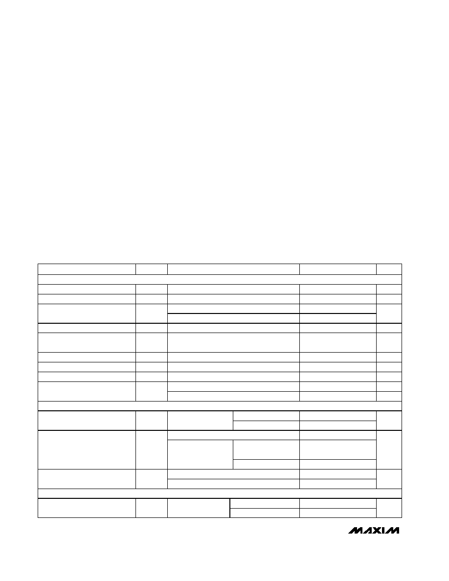
PARAMETER
SYMBOL
CONDITIONS
MIN
TYP
MAX
UNITS
INPUT (IN_+, IN_-)
Input Differential Voltage Range
VID
Guaranteed by input bias current tests
-5.2
+5.2
V
Input Common-Mode Voltage
VCM
Guaranteed by input bias current tests
VEE + 3
VCC - 2
V
TA = +25
°C
±1
±5
Input Offset Voltage
VOS
TMIN
≤ TA ≤ TMAX
±9
mV
Input Offset-Voltage Tempco
TCVOS
8
V/
°C
Input Offset-Voltage Channel
Matching
1mV
Input Bias Current
IB
VID =
±5.2V
6
20
A
Input Bias-Current Tempco
TCIB
10
nA/
°C
Input Offset Current
IOS
0.3
±5A
Differential mode (VID
≤ 10mV)
10
k
Input Resistance
RIN
Common mode (VEE + 3V)
≤ VCM ≤ (VCC - 2V)
100
M
LATCH INPUT (LE_, LE
_)
MAX9600
0.4
2.0
Latch Differential Input Voltage
VLD
Guaranteed by latch
input current
MAX9601
0.25
3.50
V
MAX9600
-2
0
VCCO_
≥ 3.5V
VCCO_
- 3.5
VCCO_
Latch Input Voltage Range
VLR
MAX9601
VCCO_
< 3.5V
0
VCCO_
V
MAX9600
5
20
Latch Input Current
ILE, ILE
MAX9601
5
20
A
HYSTERESIS INPUT (HYS_)
RHYS =
∞
0
Input-Referred Hysteresis
MAX9600/MAX9601
RHYS = 16.4k
30
mV
DC ELECTRICAL CHARACTERISTICS
(VCC = 5V, VEE = -5.2V, VCM = 0V, HYS_ = open (MAX9600/MAX9601), LE_ = low, LE_ = high (MAX9600/MAX9601), GND = 0V,
RL = 50
to -2V (MAX9600), VCCO_ = 5V, RL = 50 to 3V (MAX9601/MAX9602), TA = TMIN to TMAX. Typical values are at
TA = +25°C, unless otherwise noted.) (Note 1)
相关PDF资料 |
PDF描述 |
|---|---|
| MAX9646EUK+T | IC COMPARATOR W/REF SOT23-5 |
| MAX9648AXK+T | IC COMPARATOR GP SGL SC70-5 |
| MAX964EEE+T | IC COMPARATOR BTR 16-QSOP |
| MAX964EEE | IC COMP BEYOND-RAILS QUAD 16QSOP |
| MAX9651AUA+T | IC OPAMP VCOM DRIVE 8-UMAX-EP |
相关代理商/技术参数 |
参数描述 |
|---|---|
| MAX9610EVKIT+ | 功能描述:放大器 IC 开发工具 MAX9610 Eval Kit RoHS:否 制造商:International Rectifier 产品:Demonstration Boards 类型:Power Amplifiers 工具用于评估:IR4302 工作电源电压:13 V to 23 V |
| MAX9610FELT+ | 制造商:Maxim Integrated Products 功能描述:1?A ?DFN/SC70 LITHIUM-ION BATTERY - Rail/Tube |
| MAX9610FELT+T | 功能描述:电流灵敏放大器 1uA Li-Ion Battery Current-Sense Amp RoHS:否 制造商:Texas Instruments 通道数量: 共模抑制比(最小值):110 dB 输入补偿电压:80 uV 电源电压-最大:5.5 V 电源电压-最小:2.7 V 电源电流:350 uA 最大工作温度:+ 125 C 最小工作温度:- 40 C 安装风格:SMD/SMT 封装 / 箱体:VQFN-16 封装:Reel |
| MAX9610FEXK+ | 制造商:Maxim Integrated Products 功能描述:1 A DFN/SC70 LITHIUM-ION BATTERY PRECISION CURRENT-SENSE AM - Rail/Tube |
| MAX9610FEXK+T | 功能描述:电流灵敏放大器 1uA Li-Ion Battery Current-Sense Amp RoHS:否 制造商:Texas Instruments 通道数量: 共模抑制比(最小值):110 dB 输入补偿电压:80 uV 电源电压-最大:5.5 V 电源电压-最小:2.7 V 电源电流:350 uA 最大工作温度:+ 125 C 最小工作温度:- 40 C 安装风格:SMD/SMT 封装 / 箱体:VQFN-16 封装:Reel |
发布紧急采购,3分钟左右您将得到回复。