- 您现在的位置:买卖IC网 > PDF目录3368 > MAX9610TEXK+T (Maxim Integrated Products)IC AMP CURR SENSE 25V/V SC70-5 PDF资料下载
参数资料
| 型号: | MAX9610TEXK+T |
| 厂商: | Maxim Integrated Products |
| 文件页数: | 8/11页 |
| 文件大小: | 0K |
| 描述: | IC AMP CURR SENSE 25V/V SC70-5 |
| 产品培训模块: | Lead (SnPb) Finish for COTS Obsolescence Mitigation Program |
| 标准包装: | 2,500 |
| 放大器类型: | 电流检测 |
| 电路数: | 1 |
| -3db带宽: | 170kHz |
| 电压 - 输入偏移: | 100µV |
| 电流 - 电源: | 0.75µA |
| 电压 - 电源,单路/双路(±): | 1.6 V ~ 5.5 V |
| 工作温度: | -40°C ~ 85°C |
| 安装类型: | 表面贴装 |
| 封装/外壳: | 6-TSSOP(5 引线),SC-88A,SOT-353 |
| 供应商设备封装: | SC-70-5 |
| 包装: | 带卷 (TR) |
MAX9610
1A, DFN/SC70, Lithium-Ion Battery,
Precision Current-Sense Amplifier
6
_______________________________________________________________________________________
Detailed Description
The MAX9610 family of unidirectional high-side, cur-
rent-sense amplifiers features a 1.6V to 5.5V input com-
mon-mode range. The input range is excellent for
monitoring the current of a single-cell lithium-ion battery
(Li+), which at full charge is 4.2V, typically 3.6V in nor-
mal use, and less than 2.9V when ready to be
recharged. The MAX9610 is ideal for many battery-
powered, handheld devices because it uses only 1μA
quiescent supply current to extend battery life. The
MAX9610 monitors current through a current-sense
resistor and amplifies the voltage across that resistor.
See the
Typical Operating Circuit on page 1.
The MAX9610 is a unidirectional current-sense amplifier
that has a well-established history. An op amp is used
to force the current through an internal gain resistor at
RS+ that has a value of R1, such that its voltage drop
equals the voltage drop across an external sense resis-
tor, RSENSE. There is an internal resistor at RS- with the
same value as R1 to minimize offset voltage. The cur-
rent through R1 is sourced by a pFET. Its drain current
is the same as its source current that flows through a
second gain resistor, ROUT. This produces an output
voltage, VOUT, whose magnitude is ILOAD x RSENSE x
ROUT/R1. The gain accuracy is based on the matching
of the two gain resistors R1 and ROUT (see Table 1).
Total gain = 25V/V for the MAX9610T, 50V/V for the
MAX9610F, and 100V/V for the MAX9610H.
Applications Information
Choosing the Sense Resistor
Choose RSENSE based on the following criteria.
Voltage Loss
A high RSENSE value causes the power-source voltage
to drop due to IR loss. For minimal voltage loss, use the
lowest RSENSE value.
OUT Swing vs. VRS+ and VSENSE
The MAX9610 is unique since the supply voltage is the
input common-mode voltage (the average voltage at
RS+ and RS-). There is no separate VCC supply voltage
input. Therefore, the OUT voltage swing is limited by
the minimum voltage at RS+.
VOUT(MAX) = VRS+(MAX) - VSENSE(MAX) - VOH
and
VSENSE full scale should be less than VOUT/gain at the
minimum RS+ voltage. For best performance with a
3.6V supply voltage, select RSENSE to provide approxi-
mately 120mV (gain of 25V/V), 60mV (gain of 50V/V), or
30mV (gain of 100V/V) of sense voltage for the full-
scale current in each application. These can be
increased by use of a higher minimum input voltage.
Accuracy
In the linear region (VOUT < VOUT(MAX)), there are two
components to accuracy: input offset voltage (VOS) and
Gain Error (GE). The MAX9610 has VOS = 500μV (max)
and Gain Error of 0.5% (max). Use the following linear
equation to calculate total error.
VOUT = (Gain ± GE) x VSENSE ± (Gain x VOS)
A high RSENSE value allows lower currents to be mea-
sured more accurately because offsets are less signifi-
cant when the sense voltage is larger.
Efficiency and Power Dissipation
At high current levels, the I2R loss in RSENSE can be
significant. Take this into consideration when choosing
the resistor value and its power dissipation (wattage)
rating. Also, the sense resistor’s value might drift if it is
allowed to heat up excessively. The precision VOS of
the MAX9610 allows the use of small sense resistors to
reduce power dissipation and reduce hot spots.
R
V
GI
SENSE
OUT
LOAD MAX
=
×
()
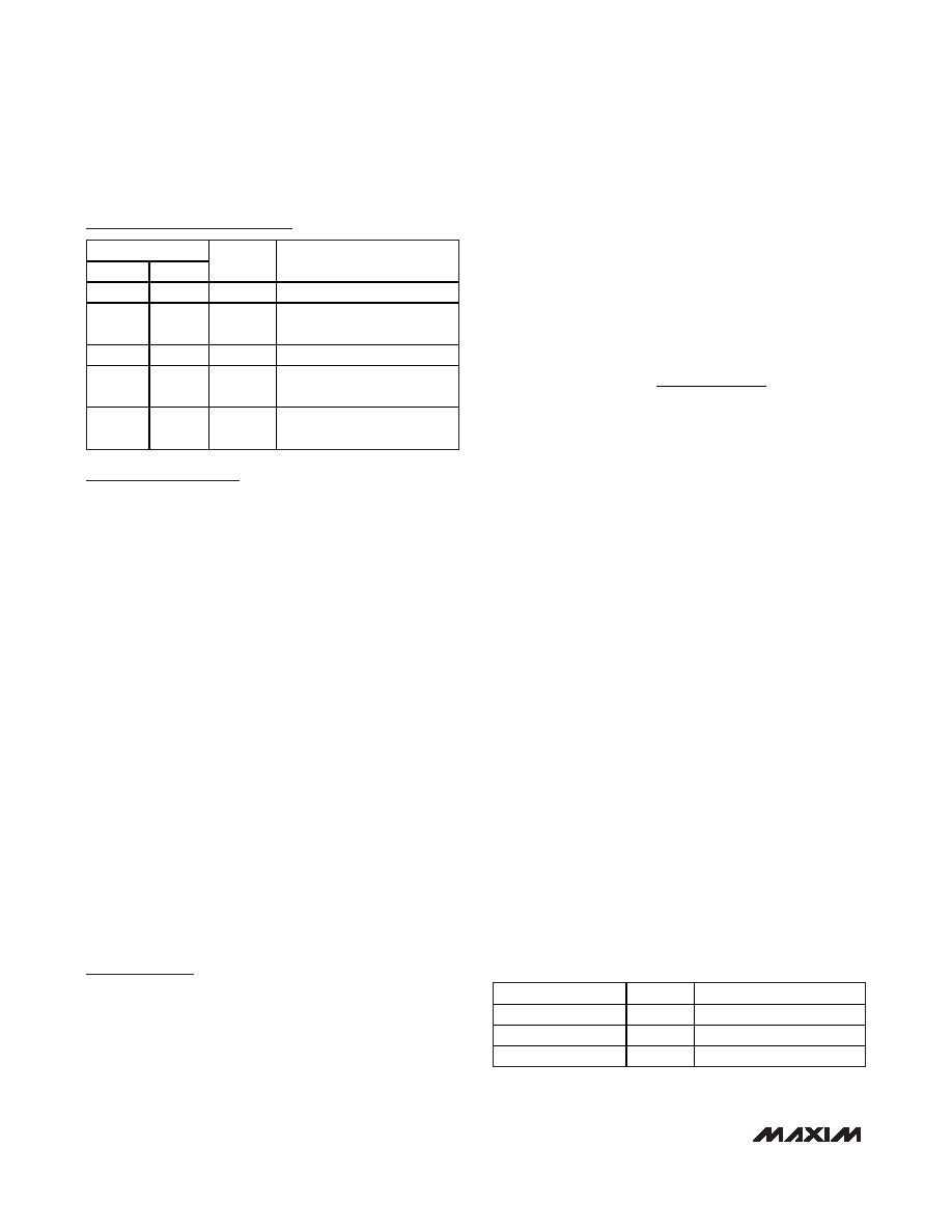
Pin Description
PIN
DFN
SC70
NAME
FUNCTION
1
1, 2
GND
Ground
2, 5
—
N.C.
No Connection. Not internally
connected.
3
OUT
Output
4
RS-
Load-Side Connection to
External Sense Resistor
6
5
RS+
Power-Side Connection to
External Sense Resistor
GAIN (V/V)
R1 (
Ω)ROUT (Ω)
100
10k
50
200
10k
25
400
10k
Table 1. MAX9610, Internal Gain Setting
Resistors (Typical Values)
相关PDF资料 |
PDF描述 |
|---|---|
| LSP1300AJR-S | LED SHUNT PROTECTOR 13V SMD |
| 2JQ 5-R | FUSE 5A 350V FAST 2AG 2JQ |
| TLV2264AINE4 | IC OPAMP GP R-R 710KHZ 14DIP |
| 5MF 200-R | FUSE 200MA 250VAC 5X20 FAST |
| 5MF 6-R | FUSE 6A 125V F UL 5X20 5MF |
相关代理商/技术参数 |
参数描述 |
|---|---|
| MAX9611AUB+ | 功能描述:电流灵敏放大器 iSense + ADC + I2C RoHS:否 制造商:Texas Instruments 通道数量: 共模抑制比(最小值):110 dB 输入补偿电压:80 uV 电源电压-最大:5.5 V 电源电压-最小:2.7 V 电源电流:350 uA 最大工作温度:+ 125 C 最小工作温度:- 40 C 安装风格:SMD/SMT 封装 / 箱体:VQFN-16 封装:Reel |
| MAX9611AUB+T | 功能描述:电流灵敏放大器 iSense + ADC + I2C RoHS:否 制造商:Texas Instruments 通道数量: 共模抑制比(最小值):110 dB 输入补偿电压:80 uV 电源电压-最大:5.5 V 电源电压-最小:2.7 V 电源电流:350 uA 最大工作温度:+ 125 C 最小工作温度:- 40 C 安装风格:SMD/SMT 封装 / 箱体:VQFN-16 封装:Reel |
| MAX9611EVKIT+ | 功能描述:放大器 IC 开发工具 MAX9611 Eval Kit RoHS:否 制造商:International Rectifier 产品:Demonstration Boards 类型:Power Amplifiers 工具用于评估:IR4302 工作电源电压:13 V to 23 V |
| MAX9611PMB1# | 功能描述:放大器 IC 开发工具 MAX9611 Peripheral Module RoHS:否 制造商:International Rectifier 产品:Demonstration Boards 类型:Power Amplifiers 工具用于评估:IR4302 工作电源电压:13 V to 23 V |
| MAX9612AUB+ | 功能描述:电流灵敏放大器 iSense + ADC + I2C RoHS:否 制造商:Texas Instruments 通道数量: 共模抑制比(最小值):110 dB 输入补偿电压:80 uV 电源电压-最大:5.5 V 电源电压-最小:2.7 V 电源电流:350 uA 最大工作温度:+ 125 C 最小工作温度:- 40 C 安装风格:SMD/SMT 封装 / 箱体:VQFN-16 封装:Reel |
发布紧急采购,3分钟左右您将得到回复。