- 您现在的位置:买卖IC网 > PDF目录3524 > MAX9611AUB+ (Maxim Integrated Products)IC 12BIT ADC OPAMP COMPAR 10UMAX PDF资料下载
参数资料
| 型号: | MAX9611AUB+ |
| 厂商: | Maxim Integrated Products |
| 文件页数: | 10/20页 |
| 文件大小: | 0K |
| 描述: | IC 12BIT ADC OPAMP COMPAR 10UMAX |
| 产品培训模块: | Lead (SnPb) Finish for COTS Obsolescence Mitigation Program |
| 标准包装: | 25 |
| 放大器类型: | 电流检测 |
| 电路数: | 1 |
| 增益带宽积: | 2.5MHz |
| -3db带宽: | 4MHz |
| 电流 - 输入偏压: | 1µA |
| 电压 - 输入偏移: | 100µV |
| 电流 - 电源: | 1.6mA |
| 电流 - 输出 / 通道: | 15mA |
| 电压 - 电源,单路/双路(±): | 2.7 V ~ 5.5 V |
| 工作温度: | -40°C ~ 125°C |
| 安装类型: | 表面贴装 |
| 封装/外壳: | 10-TFSOP,10-MSOP(0.118",3.00mm 宽) |
| 供应商设备封装: | 10-uMAX |
| 包装: | 管件 |
High-Side, Current-Sense Amplifiers with
12-Bit ADC and Op Amp/Comparator
MAX9611/MAX9612
18 _____________________________________________________________________________________
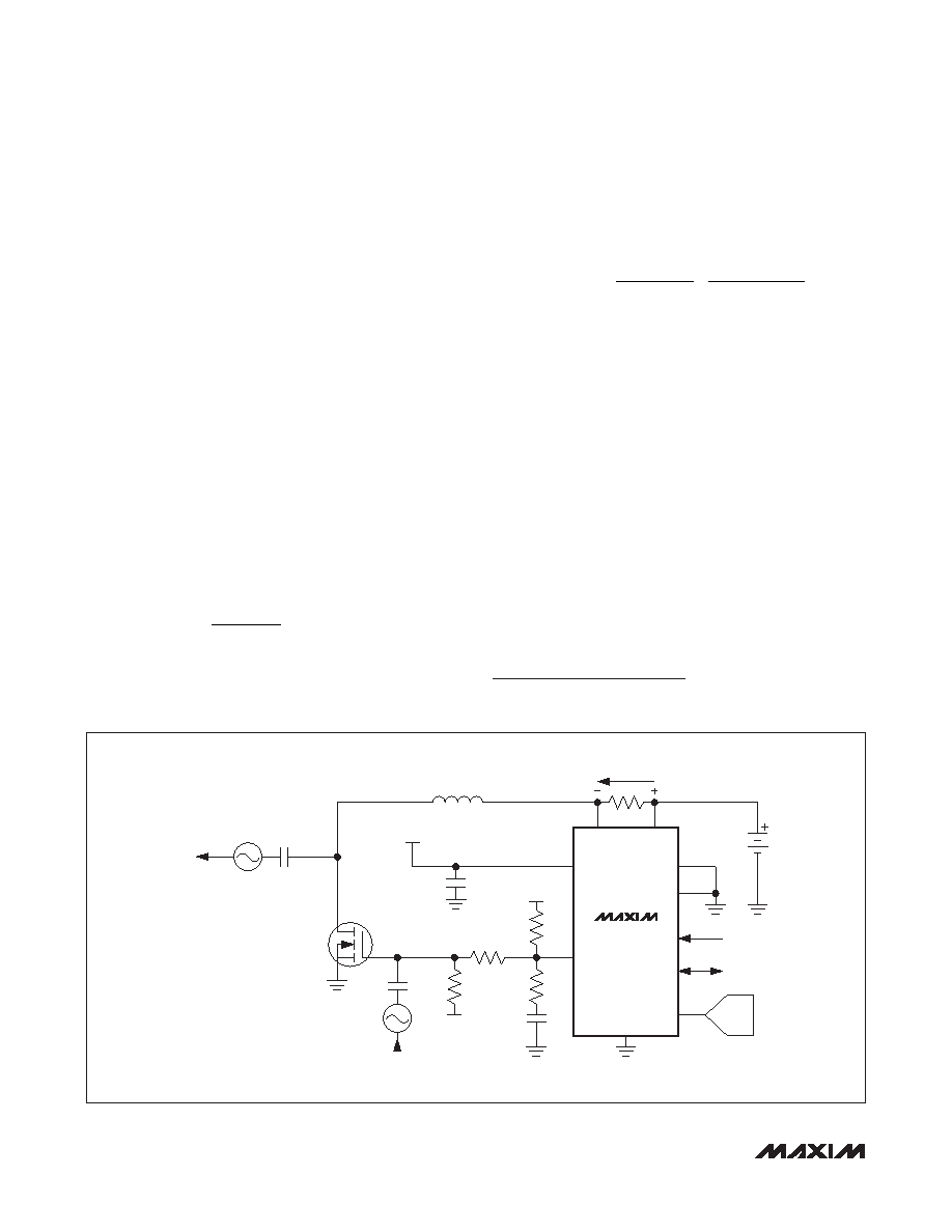
Base-Station PA Gain Control
While the MAX9611 is designed to control high-side
pFETs, the MAX9612 can be similarly used to control
low-side nFETs. For example the MAX9612 can be used
to control the DC bias point of power amplifier LDMOS
or GaN nFETs in base-station applications. The circuit
shown in Figure 4 also allows the option to apply nega-
tive bias voltages to the PA FET, which is required for
certain types of transistors for proper operation.
In the circuit shown, the nFET is in a linear mode of
operation to allow it to amplify high-frequency RF sig-
nals, while the MAX9612 sets the DC operating point.
The gain of the FET can be varied by changing its drain
current. This operating point can be varied by an exter-
nal DAC voltage that feeds the SET pin.
VNEG and VCLAMP together with R1, R2, and R3 set the
DC bias point limits for the PA transistor. VCLAMP is a
suitable positive voltage and VNEG is a suitable nega-
tive voltage. When VOUT = 0V, the gate voltage of the
PA FET is:
(
)
×
=
+
NEG
OUT
V
R2
V
R1 R2
When the OUT open-dran transistor is off, the gate volt-
age of the PA FET is:
(
)
+
=
+
++
NEG
CLAMP
GATE
V
R2 R3
V
R1
V
R1 R2 R3
RCOMP and CCOMP connected to the OUT pin compen-
sate the internal amplifier. Choose a corner frequency
of 100kHz.
Choose suitable RSENSE as required for the application.
The inductor isolates the DC measuring point of current
from the high-frequency AC signals through the PA FET,
as well as helping with the high-frequency gain.
Power-Supply Bypassing and Grounding
The MAX9611/MAX9612 share a common ground pin
for both the analog and digital on-chip circuitry. It is
therefore very important to properly bypass the VCC to
GND, and to have a solid low-noise ground plane on the
circuit board so as to minimize ground bounce. Bypass
VCC to GND with low ESR 0.1FF in parallel with a 4.7FF
ceramic capacitors to GND placed as close as possible
to the device.
Figure 4. Base-Station PA Gain Control
Chip Information
PROCESS: BiCMOS
MAX9612
CIN
VCC
RS-
RS+
A0
A1
SET
OUT
2.7V TO 5.5V
VNEG
VCLAMP
(OUTPUT SET TO OP-AMP MODE)
BASE-STATION PA GAIN CONTROL
RFIN
GND
I2C CLOCK
INPUT
I2C DATA
INPUT/OUTPUT
SCL
SDA
10-BIT
DAC
RCOMP
R2
R1
R3
N
CCOMP
RFOUT
相关PDF资料 |
PDF描述 |
|---|---|
| LT6200IS6#TRPBF | IC OPAMP R-R I/O 165MHZ SOT23-6 |
| MAX44251AUA+ | IC AMP LNA 20V ULT PREC UMAX |
| EL5104IW-T7 | IC OP AMP HS VF 700MHZ SOT23-6 |
| LT6200IS6#TRM | IC OPAMP R-R I/O 165MHZ SOT23-6 |
| 9-146305-0-23 | CONN HEADR BRKWAY .100 23POS R/A |
相关代理商/技术参数 |
参数描述 |
|---|---|
| MAX9611AUB+ | 功能描述:电流灵敏放大器 iSense + ADC + I2C RoHS:否 制造商:Texas Instruments 通道数量: 共模抑制比(最小值):110 dB 输入补偿电压:80 uV 电源电压-最大:5.5 V 电源电压-最小:2.7 V 电源电流:350 uA 最大工作温度:+ 125 C 最小工作温度:- 40 C 安装风格:SMD/SMT 封装 / 箱体:VQFN-16 封装:Reel |
| MAX9611AUB+T | 功能描述:电流灵敏放大器 iSense + ADC + I2C RoHS:否 制造商:Texas Instruments 通道数量: 共模抑制比(最小值):110 dB 输入补偿电压:80 uV 电源电压-最大:5.5 V 电源电压-最小:2.7 V 电源电流:350 uA 最大工作温度:+ 125 C 最小工作温度:- 40 C 安装风格:SMD/SMT 封装 / 箱体:VQFN-16 封装:Reel |
| MAX9611EVKIT+ | 功能描述:放大器 IC 开发工具 MAX9611 Eval Kit RoHS:否 制造商:International Rectifier 产品:Demonstration Boards 类型:Power Amplifiers 工具用于评估:IR4302 工作电源电压:13 V to 23 V |
| MAX9611PMB1# | 功能描述:放大器 IC 开发工具 MAX9611 Peripheral Module RoHS:否 制造商:International Rectifier 产品:Demonstration Boards 类型:Power Amplifiers 工具用于评估:IR4302 工作电源电压:13 V to 23 V |
| MAX9612AUB+ | 功能描述:电流灵敏放大器 iSense + ADC + I2C RoHS:否 制造商:Texas Instruments 通道数量: 共模抑制比(最小值):110 dB 输入补偿电压:80 uV 电源电压-最大:5.5 V 电源电压-最小:2.7 V 电源电流:350 uA 最大工作温度:+ 125 C 最小工作温度:- 40 C 安装风格:SMD/SMT 封装 / 箱体:VQFN-16 封装:Reel |
发布紧急采购,3分钟左右您将得到回复。