- 您现在的位置:买卖IC网 > PDF目录2158 > MAX9611AUB+T (Maxim Integrated Products)IC 12BIT ADC OPAMP COMPAR 10UMAX PDF资料下载
参数资料
| 型号: | MAX9611AUB+T |
| 厂商: | Maxim Integrated Products |
| 文件页数: | 6/20页 |
| 文件大小: | 0K |
| 描述: | IC 12BIT ADC OPAMP COMPAR 10UMAX |
| 标准包装: | 2,500 |
| 放大器类型: | 电流检测 |
| 电路数: | 1 |
| 增益带宽积: | 2.5MHz |
| -3db带宽: | 4MHz |
| 电流 - 输入偏压: | 1µA |
| 电压 - 输入偏移: | 100µV |
| 电流 - 电源: | 1.6mA |
| 电流 - 输出 / 通道: | 15mA |
| 电压 - 电源,单路/双路(±): | 2.7 V ~ 5.5 V |
| 工作温度: | -40°C ~ 125°C |
| 安装类型: | * |
| 封装/外壳: | * |
| 供应商设备封装: | * |
| 包装: | * |
High-Side, Current-Sense Amplifiers with
12-Bit ADC and Op Amp/Comparator
MAX9611/MAX9612
14 _____________________________________________________________________________________
Slave Address
A bus master initiates communication with a slave
device by issuing a START (S) condition followed by a
slave address. When idle, the MAX9611/MAX9612 con-
tinuously wait for a START condition followed by their
slave address. When the MAX9611/MAX9612 recognize
a slave address, it is ready to accept or send data. The
MAX9611/MAX9612 offer 16 different slave addresses
using two address inputs, A1 and A0. See Table 2 for
different slave address options. The least significant bit
(LSB) of the address byte (R/W) determines whether
the master is writing to or reading from the MAX9611/
MAX9612 (R/W = 0 selects a write condition, R/W = 1
selects a read condition). After receiving the address,
the MAX9611/MAX9612 (slave) issue an acknowledge
by pulling SDA low for one clock cycle.
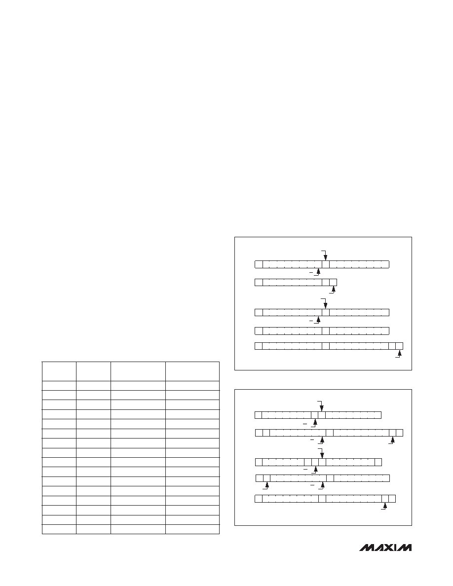
I2C Write Operation
A write operation (Figure 1) begins with the bus master
issuing a START condition followed by seven address
bits and a write bit (R/W = 0). If the address byte is
successfully received, the MAX9611/MAX9612 (slave)
issue an acknowledge (A). The master then writes to
the slave and the sequence is terminated by a STOP (P)
condition for a single write operation.
For a burst write operation, more data bytes are sent after
the register address before the transaction is terminated.
I2C Read Operation
In an I2C read operation (Figure 2), the bus master
issues a write command first by initiating a START condi-
tion followed by seven address bits, a write bit (R/W = 0)
and the 8-bit register address. The master then issues
a Repeated START (Sr) condition, followed by seven
address bits, a read bit (R/W = 1). If the address byte
is successfully received, the MAX9611/MAX9612 (slave)
issue an acknowledge (A). The master then reads from
the slave. For continuous read, the master issues an
acknowledge bit (AM) after each received byte. The
master terminates the read operation by sending a not
acknowledge (NA) bit. The MAX9611/MAX9612 then
release the data line SDA allowing the master to gener-
ate a STOP condition.
Table 2. MAX9611/MAX9612 Address
Description
Figure 1. I2C Write Operation
Figure 2. I2C Read Operation
A1
A0
DEVICE WRITE
ADDRESS (hex)
DEVICE READ
ADDRESS (hex)
0
0xE0
0xE1
0
1/3 x VCC
0xE2
0xE3
0
2/3 x VCC
0xE4
0xE5
0
VCC
0xE6
0xE7
1/3 x VCC
0
0xE8
0xE9
1/3 x VCC 1/3 x VCC
0xEA
0xEB
1/3 x VCC 2/3 x VCC
0xEC
0xED
1/3 x VCC
VCC
0xEE
0xEF
2/3 x VCC
0
0xF0
0xF1
2/3 x VCC 1/3 x VCC
0xF2
0xF3
2/3 x VCC 2/3 x VCC
0xF4
0xF5
2/3 x VCC
VCC
0xF6
0xF7
VCC
0
0xF8
0xF9
VCC
1/3 x VCC
0xFA
0xFB
VCC
2/3 x VCC
0xFC
0xFD
VCC
0xFE
0xFF
SINGLE WRITE
BURST WRITE
REGISTER ADDRESS
SLAVE ADDRESS
S0 A
AP
DATA
AA P
ACKNOWLEDGE FROM
MAX9611/MAX9612
R/W
STOP
REGISTER ADDRESS
SLAVE ADDRESS
S0 A
DATA 2
DATA 1
AA
DATA N
DATA 3
AA
ACKNOWLEDGE FROM
MAX9611/MAX9612
R/W
STOP
ACKNOWLEDGE FROM
MAX9611/MAX9612
ACKNOWLEDGE FROM
FROM MASTER
SINGLE READ
REGISTER ADDRESS
SLAVE ADDRESS
DATA
S
ASr1
R/W
0A
NO READ-ACKNOWLEDGE
FROM MASTER
R/W
AAMP
ACKNOWLEDGE FROM
MAX9611/MAX9612
BURST READ
REPEAT
START
REGISTER ADDRESS
SLAVE ADDRESS
DATA
S
ASr1
R/W
0A
R/W
A
DATA N
AM
NA P
AM
DATA
相关PDF资料 |
PDF描述 |
|---|---|
| MAX9614AXT+T | IC OPAMP GP RR 2.8MHZ LP SC70-6 |
| MAX9615AXA+T | IC OPAMP RRIO 2.8MHZ DUAL SC70-8 |
| MAX9619AXT+T | IC OP AMP RRIO LOW POWER SC70-6 |
| MAX9623AXK+T | IC OPAMP RAIL-TO-RAIL SC70-5 |
| MAX9627ATC+ | IC DIFF AMP/DRIVER LN 12TQFN |
相关代理商/技术参数 |
参数描述 |
|---|---|
| MAX9611EVKIT+ | 功能描述:放大器 IC 开发工具 MAX9611 Eval Kit RoHS:否 制造商:International Rectifier 产品:Demonstration Boards 类型:Power Amplifiers 工具用于评估:IR4302 工作电源电压:13 V to 23 V |
| MAX9611PMB1# | 功能描述:放大器 IC 开发工具 MAX9611 Peripheral Module RoHS:否 制造商:International Rectifier 产品:Demonstration Boards 类型:Power Amplifiers 工具用于评估:IR4302 工作电源电压:13 V to 23 V |
| MAX9612AUB+ | 功能描述:电流灵敏放大器 iSense + ADC + I2C RoHS:否 制造商:Texas Instruments 通道数量: 共模抑制比(最小值):110 dB 输入补偿电压:80 uV 电源电压-最大:5.5 V 电源电压-最小:2.7 V 电源电流:350 uA 最大工作温度:+ 125 C 最小工作温度:- 40 C 安装风格:SMD/SMT 封装 / 箱体:VQFN-16 封装:Reel |
| MAX9612AUB+T | 功能描述:电流灵敏放大器 iSense + ADC + I2C RoHS:否 制造商:Texas Instruments 通道数量: 共模抑制比(最小值):110 dB 输入补偿电压:80 uV 电源电压-最大:5.5 V 电源电压-最小:2.7 V 电源电流:350 uA 最大工作温度:+ 125 C 最小工作温度:- 40 C 安装风格:SMD/SMT 封装 / 箱体:VQFN-16 封装:Reel |
| MAX9613AXT+ | 制造商:Maxim Integrated Products 功能描述: 制造商:Maxim Integrated Products 功能描述:RAIL-RAIL PRECISION 3MHZ OP AMP - Rail/Tube |
发布紧急采购,3分钟左右您将得到回复。