- 您现在的位置:买卖IC网 > PDF目录3448 > MAX9632ASA+ (Maxim Integrated Products)IC OPAMP GP 55MHZ LN 8SOIC PDF资料下载
参数资料
| 型号: | MAX9632ASA+ |
| 厂商: | Maxim Integrated Products |
| 文件页数: | 14/15页 |
| 文件大小: | 0K |
| 描述: | IC OPAMP GP 55MHZ LN 8SOIC |
| 产品培训模块: | Lead (SnPb) Finish for COTS Obsolescence Mitigation Program |
| 标准包装: | 1 |
| 放大器类型: | 通用 |
| 电路数: | 1 |
| 输出类型: | 满摆幅 |
| 转换速率: | 30 V/µs |
| 增益带宽积: | 55MHz |
| 电流 - 输入偏压: | 30nA |
| 电压 - 输入偏移: | 30µV |
| 电流 - 电源: | 3.9mA |
| 电流 - 输出 / 通道: | 560µA |
| 电压 - 电源,单路/双路(±): | 4.5 V ~ 36 V,±2.25 V ~ 18 V |
| 工作温度: | -40°C ~ 125°C |
| 安装类型: | 表面贴装 |
| 封装/外壳: | 8-SOIC(0.154",3.90mm 宽) |
| 供应商设备封装: | 8-SOIC |
| 包装: | 管件 |
8
Maxim Integrated
36V, Precision, Low-Noise,
Wide-Band Amplifier
MAX9632
Detailed Description
The MAX9632 is designed in a new 36V, high-speed
complementary BiCMOS process that is optimized for
excellent AC dynamic performance combined with high-
voltage operation.
The IC offers precision, high-bandwidth, ultra-low noise
and exceptional distortion performance.
The IC is unity-gain stable and operates either with
single-supply voltage up to 36V or with dual supplies up
to Q18V.
Applications Information
Operating Supply Voltage
The IC can operate with dual supplies from Q2.25V to
Q
18V or with a single supply from +4.5V to +36V with
respect to ground. Even though the IC supports high-
voltage operation with excellent performance, the device
can also operate in very popular applications at 5V.
Low Noise and Low Distortion
The IC is designed for extremely low-noise applications
such as professional audio equipment, very high perfor-
mance instrumentations, automated test equipment, and
medical imaging. The low noise, combined with fast set-
tling time, makes it ideal to drive high-resolution sigma-
delta or SARs analog-to-digital converters.
The IC is also designed for ultra-low-distortion perfor-
mance. THD specifications in the Electrical Characteristics
table and Typical Operating Characteristics are calcu-
lated up to the fifth harmonic. Even when driving high-
voltage swing up to 10VP-P, the IC maintains excellent low
distortion operation over and above 100kHz of bandwidth.
Rail-to-Rail Output Stage
The output stage swings to within 50mV (typ) of either
power-supply rail with a 10kI load and provides a
55MHz GBW with a 30V/s slew rate. The device is
unity-gain stable and can drive a 100pF capacitive
load without compromising stability. Stability with higher
capacitive loads can be improved by adding an isola-
tion resistor in series with the op-amp output. This resis-
tor improves the circuit’s phase margin by isolating the
load capacitor from the amplifier’s output. The Typical
Operating Characteristics show a profile of the isolation
resistor and capacitive load values that maintain the
device into the stable region.
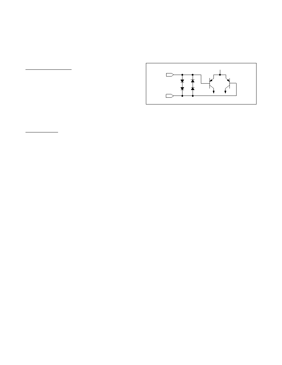
Input Differential Voltage Protection
During normal op-amp operation, the inverting and nonin-
verting inputs of the IC are at essentially the same voltage.
However, either due to fast input voltage transients or
other fault conditions, these inputs can be forced to be
at two different voltages.
Internal back-to-back diodes protect the inputs from an
excessive differential voltage (Figure 1). Therefore, IN+
and IN- can be any voltage within the range shown in the
Absolute Maximum Ratings section. Note the protection
time is still dependent on the package thermal limits.
If the input signal is fast enough to create the internal
diodes’ forward bias condition, the input signal current
must be limited to 20mA or less. If the input signal cur-
rent is not inherently limited, an input series resistor can
be used to limit the signal input current. Care should be
taken in choosing the input series resistor value, since it
degrades the low-noise performance of the device.
Shutdown
The shutdown is referenced to the positive supply. See
the Electrical Characteristics table for the proper levels
of functionality. A high level (above VCC - 0.35V) disables
the op amp and puts the output into a high-impedance
state. A low level (below VCC - 3V) enables the device. As
an example, if the op amp is powered with dual supplies
of Q15V, the device is enabled when shutdown is at or
below 12V. The device is disabled when shutdown is at
or above 14.65V. If the op amp is powered with a single
supply of 36V, the device is enabled when shutdown is at
or below 33V. The device is disabled when shutdown is at
or above 35.65V. This input must be connected to a valid
high or low voltage and should not be left disconnected.
Power Supplies and Layout
The MAX9632 can operate with dual supplies from
Q
2.25V to Q18V or with a single supply from +4.5V to
+36V with respect to ground. When used with dual
supplies, bypass both VCC and VEE with their own
0.1FF capacitor to ground. When used with a single
supply, bypass VCC with a 0.1FF capacitor to ground.
Figure 1. Input Protection Circuit
相关PDF资料 |
PDF描述 |
|---|---|
| TSM-107-01-T-DV-TR | CONN HEADER 14POS .100" DBL SMD |
| BK/C515-1.5-R | FUSE 1.5A 250V T-LAG GLASS C515 |
| AD8032BR-REEL7 | IC OPAMP VF R-R DUAL LP 8SOIC |
| BK/C515-600-R | FUSE 600MA 250V T-LAG GLASS C515 |
| MAX4218EEE+ | IC OP AMP R-R W/ENABLE 16QSOP |
相关代理商/技术参数 |
参数描述 |
|---|---|
| MAX9632ASA+ | 功能描述:运算放大器 - 运放 36V Precision Wide-Band Amp RoHS:否 制造商:STMicroelectronics 通道数量:4 共模抑制比(最小值):63 dB 输入补偿电压:1 mV 输入偏流(最大值):10 pA 工作电源电压:2.7 V to 5.5 V 安装风格:SMD/SMT 封装 / 箱体:QFN-16 转换速度:0.89 V/us 关闭:No 输出电流:55 mA 最大工作温度:+ 125 C 封装:Reel |
| MAX9632ASA+T | 功能描述:运算放大器 - 运放 36V Precision Wide-Band Amp RoHS:否 制造商:STMicroelectronics 通道数量:4 共模抑制比(最小值):63 dB 输入补偿电压:1 mV 输入偏流(最大值):10 pA 工作电源电压:2.7 V to 5.5 V 安装风格:SMD/SMT 封装 / 箱体:QFN-16 转换速度:0.89 V/us 关闭:No 输出电流:55 mA 最大工作温度:+ 125 C 封装:Reel |
| MAX9632ATA+ | 制造商:Maxim Integrated Products 功能描述:OPERATIONAL AMPLIFIER - Rail/Tube |
| MAX9632ATA+T | 功能描述:运算放大器 - 运放 36V Precision Wide-Band Amp RoHS:否 制造商:STMicroelectronics 通道数量:4 共模抑制比(最小值):63 dB 输入补偿电压:1 mV 输入偏流(最大值):10 pA 工作电源电压:2.7 V to 5.5 V 安装风格:SMD/SMT 封装 / 箱体:QFN-16 转换速度:0.89 V/us 关闭:No 输出电流:55 mA 最大工作温度:+ 125 C 封装:Reel |
| MAX9632AUA+ | 功能描述:运算放大器 - 运放 RoHS:否 制造商:STMicroelectronics 通道数量:4 共模抑制比(最小值):63 dB 输入补偿电压:1 mV 输入偏流(最大值):10 pA 工作电源电压:2.7 V to 5.5 V 安装风格:SMD/SMT 封装 / 箱体:QFN-16 转换速度:0.89 V/us 关闭:No 输出电流:55 mA 最大工作温度:+ 125 C 封装:Reel |
发布紧急采购,3分钟左右您将得到回复。