- 您现在的位置:买卖IC网 > PDF目录16895 > MAX9638EVKIT+ (Maxim Integrated Products)KIT EVAL FOR MAX9638 PDF资料下载
参数资料
| 型号: | MAX9638EVKIT+ |
| 厂商: | Maxim Integrated Products |
| 文件页数: | 9/16页 |
| 文件大小: | 0K |
| 描述: | KIT EVAL FOR MAX9638 |
| 产品培训模块: | Lead (SnPb) Finish for COTS Obsolescence Mitigation Program |
| 标准包装: | 1 |
| 每 IC 通道数: | 2 - 双 |
| 放大器类型: | 通用 |
| 输出类型: | 满摆幅 |
| 转换速率: | 0.9 V/µs |
| 电流 - 输出 / 通道: | 55mA |
| 工作温度: | -40°C ~ 125°C |
| 电流供应(主 IC): | 36µA |
| 电压 - 电源,单路/双路(±): | 3.3V |
| 板类型: | 完全填充 |
| 已供物品: | 板 |
| 已用 IC / 零件: | MAX9636 |
3V/5V Low-Power, Low-Noise, CMOS,
Rail-to-Rail I/O Op Amps
MAX9636/MAX9637/MAX9638
2
Stresses beyond those listed under “Absolute Maximum Ratings” may cause permanent damage to the device. These are stress ratings only, and functional
operation of the device at these or any other conditions beyond those indicated in the operational sections of the specifications is not implied. Exposure to absolute
maximum rating conditions for extended periods may affect device reliability.
VDD, SHDN to VSS ..................................................-0.3V to +6V
IN+, IN-, OUT ....................................GND - 0.3V to VDD + 0.3V
Continuous Input Current (any pins)............................... Q20mA
Output Short Circuit to VDD or VSS Duration .......................... 5s
Thermal Limits (Note 1)
Multiple Layer PCB
Continuous Power Dissipation (TA = +70NC)
6-Pin SC70 (derate 3.1mW/°C above +70NC) ............245mW
B
JA.......................................................................326.5°C/W
B
JC .........................................................................115°C/W
8-Pin SC70 (derate 3.1mW/NC above +70NC).............245mW
B
JA .........................................................................326°C/W
B
JC .........................................................................115NC/W
10-Pin UTQFN (derate 7mW/NC above +70NC)........558.7mW
B
JA ......................................................................143.2NC/W
B
JC.........................................................................20.1NC/W
Operating Temperature Range........................ -40NC to +125NC
Junction Temperature ....................................................+150NC
Lead Temperature (soldering 10s) .................................+300NC
Soldering Temperature (reflow) ......................................+260NC
ELECTRICAL CHARACTERISTICS
(VDD = 3.3V, VSS = 0V, VIN+ = VIN- = VCM = VDD/2, RL = 10kI to VDD/2, SHDN = VDD, TA = -40NC to +125NC. Typical values are
at TA = +25NC, unless otherwise noted.) (Note 2)
ABSOLUTE MAXIMUM RATINGS
Note 1: Package thermal resistances were obtained using the method described in JEDEC specification JESD51-7, using a four-
layer board. For detailed information on package thermal considerations, refer to www.maxim-ic.com/thermal-tutorial.
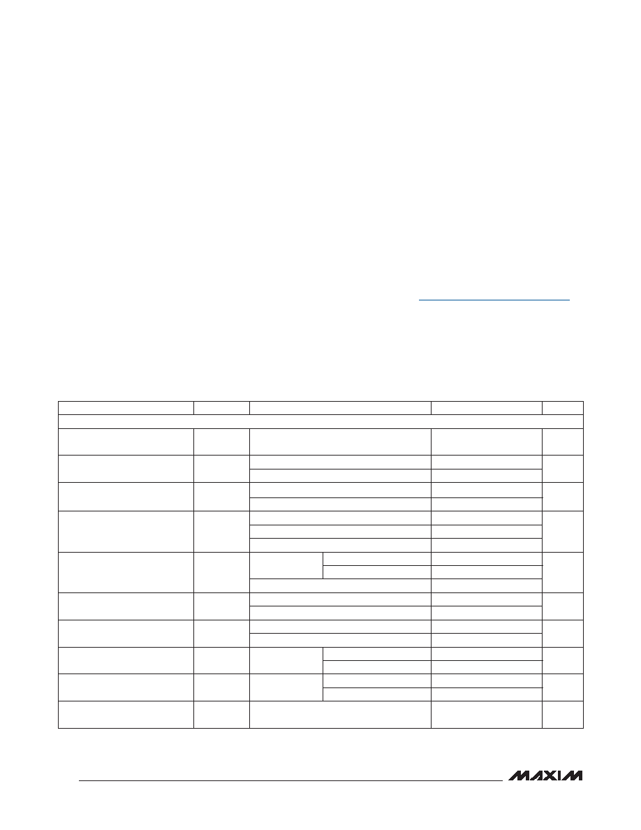
PARAMETER
SYMBOL
CONDITIONS
MIN
TYP
MAX
UNITS
DC CHARACTERISTICS
Input Voltage Range
VIN+, VIN- Guaranteed by CMRR
VSS -
0.1
VDD +
0.1
V
Input Offset Voltage
VOS
TA = +25NC
0.01
2.2
mV
TA = -40NC to +125NC
3.5
Input Offset Voltage Drift
(Note 3)
TCVOS
MAX9636 only
7
F
V/NC
MAX9637, MAX9638 only
10
Input Bias Current (Note 3)
IB
TA = +25NC
±0.1
±0.8
pA
TA = -40NC to +85NC
±50
TA = -40NC to +125NC
±800
Common-Mode Rejection Ratio
CMRR
VSS < VCM <
(VDD - 1.4V)
TA = +25NC
72
86
dB
TA = -40NC to +125NC
68
(VSS - 0.1V) < VCM < (VDD + 0.1V)
58
77
Open-Loop Gain
AOL
VOUT = 0.25V from rails
104
124
dB
VOUT = 0.4V from rails, RL = 600I
100
120
Output Short-Circuit Current
ISC
Short to VDD
55
mA
Short to VSS
40
Output Voltage Low
VOL
VOUT
RL = 10kI
0.014
0.03
V
RL = 600I
0.044
0.08
Output Voltage High
VOH
VDD - VOUT
RL = 10kI
0.019
0.04
V
RL = 600I
0.057
0.1
Output Leakage in Shutdown
SHDN = VSS, VOUT = 0V to VDD (MAX9636,
MAX9638 only)
0.01
1
F
A
相关PDF资料 |
PDF描述 |
|---|---|
| VE-B6Y-EW | CONVERTER MOD DC/DC 3.3V 66W |
| LM4040AEX3-2.5+T | IC VREF SHUNT PREC 2.5V SC-70-3 |
| TCSD-10-S-02.00-01-N | CABLE ASSEM 2MM 20POS SGL END 2" |
| EBA24DTKD-S288 | CONN EDGECARD 48POS .125 EXTEND |
| GSC07DREI-S93 | CONN EDGECARD 14POS .100 EYELET |
相关代理商/技术参数 |
参数描述 |
|---|---|
| MAX9638EVKIT# | 功能描述:放大器 IC 开发工具 RoHS:否 制造商:International Rectifier 产品:Demonstration Boards 类型:Power Amplifiers 工具用于评估:IR4302 工作电源电压:13 V to 23 V |
| MAX9638EVKIT+ | 功能描述:放大器 IC 开发工具 MAX9638 Eval Kit RoHS:否 制造商:International Rectifier 产品:Demonstration Boards 类型:Power Amplifiers 工具用于评估:IR4302 工作电源电压:13 V to 23 V |
| MAX9639EVKIT+ | 功能描述:磁场传感器模块 RoHS:否 制造商:Olimex Ltd. 产品类型:3-Axis Magnetometer Module 接口类型:UEXT Connector 电源电流: 最大工作温度: 尺寸:29 mm x 18 mm |
| MAX963ESD | 功能描述:校验器 IC Dual Comparator RoHS:否 制造商:STMicroelectronics 产品: 比较器类型: 通道数量: 输出类型:Push-Pull 电源电压-最大:5.5 V 电源电压-最小:1.1 V 补偿电压(最大值):6 mV 电源电流(最大值):1350 nA 响应时间: 最大工作温度:+ 125 C 安装风格:SMD/SMT 封装 / 箱体:SC-70-5 封装:Reel |
| MAX963ESD+ | 功能描述:校验器 IC Dual Comparator RoHS:否 制造商:STMicroelectronics 产品: 比较器类型: 通道数量: 输出类型:Push-Pull 电源电压-最大:5.5 V 电源电压-最小:1.1 V 补偿电压(最大值):6 mV 电源电流(最大值):1350 nA 响应时间: 最大工作温度:+ 125 C 安装风格:SMD/SMT 封装 / 箱体:SC-70-5 封装:Reel |
发布紧急采购,3分钟左右您将得到回复。