- 您现在的位置:买卖IC网 > PDF目录2090 > MAX9646EUK+T (Maxim Integrated Products)IC COMPARATOR W/REF SOT23-5 PDF资料下载
参数资料
| 型号: | MAX9646EUK+T |
| 厂商: | Maxim Integrated Products |
| 文件页数: | 4/11页 |
| 文件大小: | 0K |
| 描述: | IC COMPARATOR W/REF SOT23-5 |
| 产品培训模块: | Obsolescence Mitigation Program |
| 标准包装: | 2,500 |
| 类型: | 通用 |
| 元件数: | 1 |
| 输出类型: | 推挽式 |
| 电压 - 电源,单路/双路(±): | 1 V ~ 5.5 V |
| 电流 - 输入偏压(最小值): | 15nA |
| 电流 - 静态(最大值): | 1.1µA |
| CMRR, PSRR(标准): | 53dB PSRR |
| 传输延迟(最大): | 15µs |
| 磁滞: | 0.9mV |
| 工作温度: | -40°C ~ 85°C |
| 封装/外壳: | SC-74A,SOT-753 |
| 安装类型: | 表面贴装 |
| 包装: | 带卷 (TR) |
MAX9644/MAX9645/MAX9646
Low-Power Comparators with Precision
Reference in 4-Bump UCSP
2
_______________________________________________________________________________________
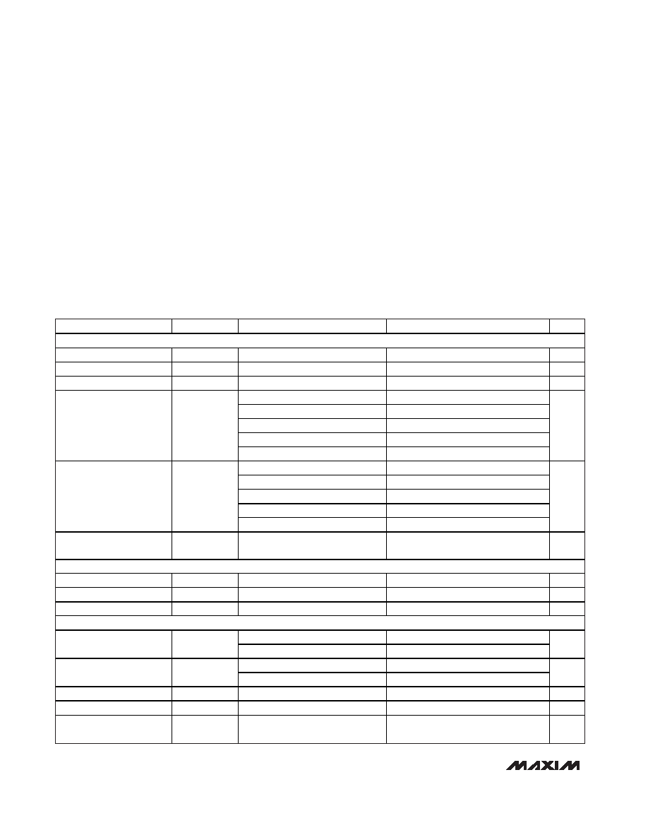
ABSOLUTE MAXIMUM RATINGS
ELECTRICAL CHARACTERISTICS
(VCC = 3.3V, RPULLUP = 10k to VPULLUP = 3.3V for MAX9644/MAX9645, TA = -40°C to +85°C. Typical values at TA = +25°C, unless
otherwise noted.) (Note 1)
Stresses beyond those listed under “Absolute Maximum Ratings” may cause permanent damage to the device. These are stress ratings only, and functional
operation of the device at these or any other conditions beyond those indicated in the operational sections of the specifications is not implied. Exposure to
absolute maximum rating conditions for extended periods may affect device reliability.
VCC, REF, IN to GND................................................-0.3V to +6V
OUT to GND (MAX9644/MAX9645)..........................-0.3V to +6V
OUT to GND (MAX9646 only) .................-0.3V to + (VCC + 0.3V)
Output Short-Circuit Current Duration ....................................10s
Input Current into Any Terminal........................................±20mA
Continuous Power Dissipation
4-Bump UCSP (derate 3.0mW/°C above +70°C) .......238 mW
5-Pin SOT23 (derate 3.9mW/°C above +70°C)...........312 mW
Operating Temperature Range ...........................-40°C to +85°C
Junction Temperature ......................................................+150°C
Storage Temperature Range .............................-65°C to +150°C
Bump Temperature (soldering) Reflow............................+235°C
Lead Temperature (soldering, 10s) .................................+300°C
Soldering Temperature (reflow) .......................................+260°C
PARAMETER
SYMBOL
CONDITIONS
MIN
TYP
MAX
UNITS
DC CHARACTERISTICS
Input Voltage Range
VIN
Guaranteed by IIN test
-0.3
+5.5
V
Input Bias Current
IIN
VIN = 0.2V to 5.5V (Note 2)
0.06
15
nA
Input Leakage Current
IIN_SHDN
VCC = 0, VIN = 5.5V (Note 2)
< 0.1
15
nA
ISINK = 50A, VCC = 1.0V
0.03
0.2
ISINK = 200A, VCC = 1.2V
0.08
0.20
ISINK = 500A, VCC = 1.8V
0.13
0.23
ISINK = 0.75mA, VCC = 3.3V
0.14
0.3
Output Voltage Low
VOL
ISINK = 1.2mA, VCC = 5.5V
0.19
0.5
V
ISOURCE = 15A, VCC = 1.0V
VCC - 0.08V
VCC - 0.2V
ISOURCE = 40A, VCC = 1.2V
VCC - 0.08V
VCC - 0.20V
ISOURCE = 180A, VCC = 1.8V
VCC - 0.15V
VCC - 0.23V
ISOURCE = 0.3mA, VCC = 3.3V
VCC - 0.13V
VCC - 0.3V
Output Voltage High
(MAX9464 Only)
VOH
ISOURCE = 0.75mA, VCC = 5.5V
VCC - 0.24V
VCC - 0.5V
V
Output Leakage Current
(MAX9644/MAX9645 Only)
IOUT_LEAKAGE
OUT = high, VPULLUP = 5.5V
(Note 2)
< 0.1
15
nA
AC CHARACTERISTICS
Propagation Delay
tPD
VOVERDRIVE = ±100mV (Note 3)
15
s
Fall Time
tF
CL = 10pF
14
ns
Rise Time
tR
CL = 10pF, MAX9646 only
30
ns
REFERENCE VOLTAGE
MAX964_EBS+
200
Input Threshold (Note 4)
VREF
MAX964_EUK+
199
mV
TA = +25°C
-1
+1
Input Threshold Error
(Note 4)
Delta-VREF
TA = -40°C to +85°C
-3.5
+3.5
%
Input Threshold Hysteresis
VHYS
TA = -40°C to +85°C (Note 5)
±0.9
mV
REF Tempco
VREF_TEMPCO
(Note 6)
6
V/°C
Power-Supply Rejection
Ratio
PSRR
VCC = 1.0V to 5.5V
40
53
dB
相关PDF资料 |
PDF描述 |
|---|---|
| MAX9648AXK+T | IC COMPARATOR GP SGL SC70-5 |
| MAX964EEE+T | IC COMPARATOR BTR 16-QSOP |
| MAX964EEE | IC COMP BEYOND-RAILS QUAD 16QSOP |
| MAX9651AUA+T | IC OPAMP VCOM DRIVE 8-UMAX-EP |
| MAX9653AUB+ | IC AMP FILTER W/SHUTDOWN 10-UMAX |
相关代理商/技术参数 |
参数描述 |
|---|---|
| MAX9646EVKIT# | 功能描述:其他开发工具 MAX9646 Eval Kit RoHS:否 制造商:Parallax 产品:ELEV-8 Hex Upgrade Kits 类型:Robotics 工具用于评估:ELEV-8 Quadcopter 工作电源电压: |
| MAX9646EVKIT+ | 功能描述:其他开发工具 MAX9646 Eval Kit RoHS:否 制造商:Parallax 产品:ELEV-8 Hex Upgrade Kits 类型:Robotics 工具用于评估:ELEV-8 Quadcopter 工作电源电压: |
| MAX9647AUK+ | 制造商:Maxim Integrated Products 功能描述:GENERAL-PURPOSE, LOW-VOLTAGE, SINGLE/DUAL/QUAD, TINYPACK COM - Rail/Tube |
| MAX9647AUK+T | 功能描述:校验器 IC Low-Power Comparator RoHS:否 制造商:STMicroelectronics 产品: 比较器类型: 通道数量: 输出类型:Push-Pull 电源电压-最大:5.5 V 电源电压-最小:1.1 V 补偿电压(最大值):6 mV 电源电流(最大值):1350 nA 响应时间: 最大工作温度:+ 125 C 安装风格:SMD/SMT 封装 / 箱体:SC-70-5 封装:Reel |
| MAX9647AXK+ | 制造商:Maxim Integrated Products 功能描述:GENERAL-PURPOSE LOW-VOLTAGE SINGLE/DUAL/QUAD TINYPACK COMPAR - Rail/Tube |
发布紧急采购,3分钟左右您将得到回复。