- 您现在的位置:买卖IC网 > PDF目录10262 > MAX9706ETX+T (Maxim Integrated Products)IC AMP AUDIO 2.3W STER+1 36TQFN PDF资料下载
参数资料
| 型号: | MAX9706ETX+T |
| 厂商: | Maxim Integrated Products |
| 文件页数: | 10/25页 |
| 文件大小: | 0K |
| 描述: | IC AMP AUDIO 2.3W STER+1 36TQFN |
| 标准包装: | 2,500 |
| 系列: | DirectDrive® |
| 类型: | D 类 |
| 输出类型: | 2-通道(立体声)带立体声耳机和超低音器 |
| 在某负载时最大输出功率 x 通道数量: | 2.3W x 3 @ 4 欧姆; 95mW x 2 @ 16 欧姆 |
| 电源电压: | 4.5 V ~ 5.5 V |
| 特点: | 消除爆音,短路保护和热保护,关闭 |
| 安装类型: | 表面贴装 |
| 供应商设备封装: | 36-TQFN 裸露焊盘(6x6) |
| 封装/外壳: | 36-WFQFN 裸露焊盘 |
| 包装: | 带卷 (TR) |
MAX9706/MAX9707
3-Channel, 2.3W, Filterless Class D Amplifiers
with Active Crossover
18
______________________________________________________________________________________
tantalum-blocking capacitors, the MAX9706 charge
pump requires two small ceramic capacitors, conserv-
ing board space, reducing cost, and improving the fre-
quency response of the headphone amplifier. See the
Output Power vs. Charge-Pump Capacitance graph in
the Typical Operating Characteristics for details on siz-
ing charge-pump capacitors. There is a low DC voltage
on the driver outputs due to amplifier offset. However,
the offset of the MAX9706 is typically 1.7mV, which,
when combined with a 32
Ω load, results in less than
53A of DC current flow to the headphones.
In addition to the cost and size disadvantages of the
DC-blocking capacitors required by conventional head-
phone amplifiers, these capacitors limit the amplifier’s
low-frequency response and can distort the audio sig-
nal (Figure 8). Previous attempts at eliminating the out-
put-coupling capacitors involved biasing the
headphone return (sleeve) to the DC bias voltage of the
headphone amplifiers. This method raises some issues:
1)
The sleeve is typically grounded to the chassis.
Using the midrail biasing approach, the sleeve
must be isolated from system ground, complicat-
ing product design.
2)
During an ESD strike, the driver’s ESD structures
are the only path to system ground. Thus, the dri-
ver must be able to withstand the full ESD strike.
When using the headphone jack as a line out to other
equipment, the bias voltage on the sleeve may conflict
with the ground potential from other equipment, result-
ing in possible damage to the drivers.
Charge Pump
The MAX9706 features a low-noise charge pump. The
switching frequency of the charge pump is one-half the
switching frequency of the Class D amplifier, regardless
of the operating mode. When SYNC_IN is driven exter-
nally, the charge pump switches at 1/2 fSYNC_IN. When
SYNC_IN = VDD, the charge pump switches with a
spread-spectrum pattern. The nominal switching fre-
quency is well beyond the audio range, and thus does
not interfere with the audio signals, resulting in an SNR of
96dB. The switch drivers feature a controlled switching
speed that minimizes noise generated by turn-on and
turn-off transients. By limiting the switching speed of the
charge pump, the di/dt noise caused by the parasitic
bond wire and trace inductance is minimized. Although
not typically required, additional high-frequency noise
attenuation can be achieved by increasing the size of the
charge-pump reservoir capacitor C2 (see the Functional
Diagram/Typical Operating Circuits). The charge pump is
active in both speaker and headphone modes.
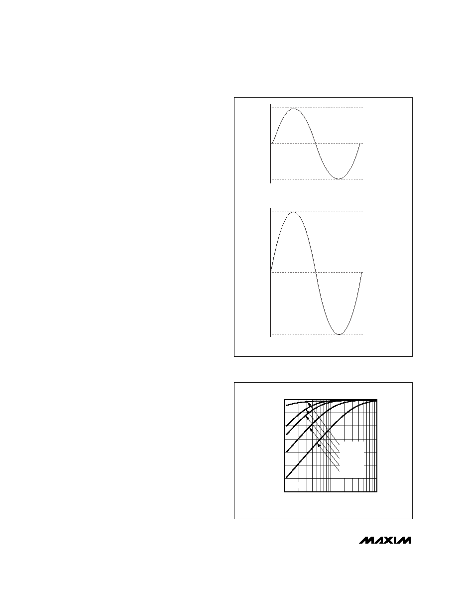
CONVENTIONAL AMPLIFIER
BIASING SCHEME
DirectDrive AMPLIFIER
BIASING SCHEME
VDD
VDD / 2
GND
+VDD
SGND
-VDD
Figure 7. Traditional Amplifier Output vs. MAX9706 DirectDrive
Output
FREQUENCY (Hz)
ATTENUATION
(dB)
100
-30
-25
-20
-15
-10
-5
0
-35
10
1000
DirectDrive
330
μF
220
μF
100
μF
33
μF
RL = 16
Ω
Figure 8. Low-Frequency Rolloff
相关PDF资料 |
PDF描述 |
|---|---|
| MAX9760ETI+T | IC AMP AUDIO PWR 3W STER 28TQFN |
| MAX9760EUI+T | IC AMP AUDIO PWR 3W STER 28TSSOP |
| MAX9761EUI+T | IC AMP AUDIO PWR 3W STER 28TSSOP |
| CXS3102A188P | CONN RCPT 8POS PNL MNT PIN |
| TB6M | CONN RCPT CORD MINI 6POS MALE |
相关代理商/技术参数 |
参数描述 |
|---|---|
| MAX9706EVKIT | 功能描述:放大器 IC 开发工具 RoHS:否 制造商:International Rectifier 产品:Demonstration Boards 类型:Power Amplifiers 工具用于评估:IR4302 工作电源电压:13 V to 23 V |
| MAX9707ETX+ | 功能描述:音频放大器 Integrated Circuits (ICs) RoHS:否 制造商:STMicroelectronics 产品:General Purpose Audio Amplifiers 输出类型:Digital 输出功率: THD + 噪声: 工作电源电压:3.3 V 电源电流: 最大功率耗散: 最大工作温度: 安装风格:SMD/SMT 封装 / 箱体:TQFP-64 封装:Reel |
| MAX9707ETX+T | 功能描述:音频放大器 Integrated Circuits (ICs) RoHS:否 制造商:STMicroelectronics 产品:General Purpose Audio Amplifiers 输出类型:Digital 输出功率: THD + 噪声: 工作电源电压:3.3 V 电源电流: 最大功率耗散: 最大工作温度: 安装风格:SMD/SMT 封装 / 箱体:TQFP-64 封装:Reel |
| MAX9708ECB+D | 制造商:Maxim Integrated Products 功能描述:AUD AMP SPKR 1CH MONO/2CH STEREO 42W/21W CLS-D 64TQFP EP - Rail/Tube |
| MAX9708ECB+TD | 制造商:Maxim Integrated Products 功能描述:AUD AMP SPKR 1CH MONO/2CH STEREO 42W/21W CLS-D 64TQFP EP - Tape and Reel |
发布紧急采购,3分钟左右您将得到回复。