- 您现在的位置:买卖IC网 > PDF目录10352 > MAX9724CEBC+TG45 (Maxim Integrated Products)IC AMP AUDIO .045W STER 12UCSP PDF资料下载
参数资料
| 型号: | MAX9724CEBC+TG45 |
| 厂商: | Maxim Integrated Products |
| 文件页数: | 12/19页 |
| 文件大小: | 0K |
| 描述: | IC AMP AUDIO .045W STER 12UCSP |
| 产品培训模块: | Lead (SnPb) Finish for COTS Obsolescence Mitigation Program |
| 标准包装: | 2,500 |
| 系列: | DirectDrive® |
| 类型: | AB 类 |
| 输出类型: | 耳机,2-通道(立体声) |
| 在某负载时最大输出功率 x 通道数量: | 45mW x 2 @ 32 欧姆 |
| 电源电压: | 2.5 V ~ 5.5 V |
| 特点: | 消除爆音,短路保护和热保护,关闭 |
| 安装类型: | 表面贴装 |
| 供应商设备封装: | 12-UCSP(3x4) |
| 封装/外壳: | 12-WFBGA,WLCSP |
| 包装: | 带卷 (TR) |
| 配用: | MAX9724AEVKIT+-ND - EVALUATION KIT FOR MAX9724A/B MAX9724DEVKIT+-ND - KIT EVAL FOR MAX9724D |
MAX9724C/MAX9724D
Low RF Susceptibility DirectDrive Stereo Head-
phone Amplifier with 1.8V Compatible Shutdown
2
_______________________________________________________________________________________
ABSOLUTE MAXIMUM RATINGS
Stresses beyond those listed under “Absolute Maximum Ratings” may cause permanent damage to the device. These are stress ratings only, and functional
operation of the device at these or any other conditions beyond those indicated in the operational sections of the specifications is not implied. Exposure to
absolute maximum rating conditions for extended periods may affect device reliability.
VDD to GND ..............................................................-0.3V to +6V
PVSS to SVSS ........................................................-0.3V to +0.3V
PGND to SGND .....................................................-0.3V to +0.3V
C1P to PGND..............................................-0.3V to (VDD + 0.3V)
C1N to PGND ...........................................(PVSS - 0.3V) to +0.3V
PVSS and SVSS to PGND.........................................-6V to +0.3V
IN_ to SGND (MAX9724C) .........................-0.3V to (VDD + 0.3V)
IN_ to SGND (MAX9724D) ............(SVSS - 0.3V) to (VDD + 0.3V)
OUT_ to SVSS (Note 1) ...-0.3V to Min (VDD - SVSS + 0.3V, +9V)
OUT_ to VDD (Note 2) .....+0.3V to Max (SVSS - VDD - 0.3V, -9V)
SHDN to _GND.........................................................-0.3V to +6V
OUT_ Short Circuit to GND ........................................Continuous
Short Circuit between OUTL and OUTR ....................Continuous
Continuous Input Current into PVSS .................................260mA
Continuous Input Current (any other pin) .........................±20mA
Continuous Power Dissipation (TA = +70°C, multilayer board)
12-Bump UCSP (derate 6.5mW/°C above +70°C) ........519mW
θJA ................................................................................154 C/W
12-Pin TQFN (derate 16.7mW/°C above +70°C) .........1333mW
θJA..................................................................................60°C/W
θJC..................................................................................11°C/W
Operating Temperature Range ...........................-40°C to +85°C
Storage Temperature Range .............................-65°C to +150°C
Junction Temperature ......................................................+150°C
Lead Temperature (soldering, 10s) .................................+300°C
Bump Temperature (soldering) Reflow............................+235°C
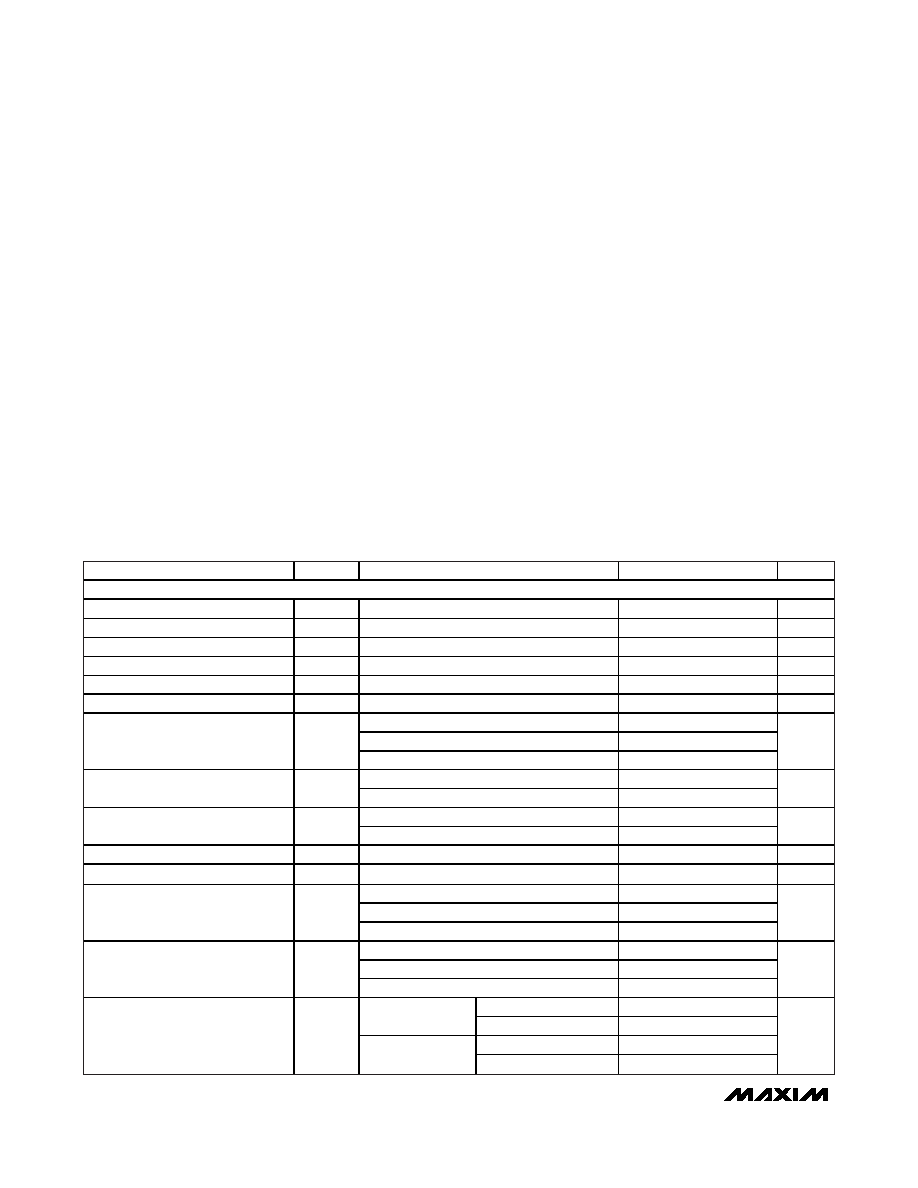
ELECTRICAL CHARACTERISTICS
(VDD = 5V, PGND = SGND, SHDN = 5V, C1 = C2 = 1F, RL = ∞, resistive load reference to ground; for MAX9724C gain = -1.5V/V
(RIN = 20kΩ, RF = 30kΩ); for MAX9724D gain = -1.5V/V (internally set), TA = -40°C to +85°C, unless otherwise noted. Typical values
are at TA = +25°C, unless otherwise noted.) (Note 3)
PARAMETER
SYMBOL
CONDITIONS
MIN
TYP
MAX
UNITS
GENERAL
Supply Voltage Range
VDD
2.5
5.5
V
Quiescent Current
ICC
3.5
5.5
mA
Shutdown Current
ISHDN
SHDN = SGND = PGND
0.1
1
A
Shutdown to Full Operation
tSON
180
s
Input Impedance
RIN
MAX9724D, measured at IN_
12
19
28
k
Ω
Output Offset Voltage
VOS
TA = +25°C (Note 4)
±1.5
±10
mV
VDD = 2.7V to 5.5V, TA = +25°C
69
86
f = 1kHz, 100mVP-P (Note 4)
80
Power-Supply Rejection Ratio
PSRR
f = 20kHz, 100mVP-P (Note 4)
65
dB
RL = 32
Ω, THD+N = 1%
30
63
Output Power (TQFN)
POUT
RL = 16
Ω, THD+N = 1%
42
mW
RL = 32
Ω, THD+N = 1%
25
45
Output Power (UCSP)
POUT
RL = 16
Ω, THD+N = 1%
35
mW
Voltage Gain
AV
MAX9724D (Note 5)
-1.52
-1.5
-1.48
V/V
Channel-to-Channel Gain Tracking
MAX9724D
±0.15
%
RL = 1k
Ω, VOUT = 2VRMS, fIN = 1kHz
0.003
RL = 32
Ω, POUT = 50mW, fIN = 1kHz
0.02
Total Harmonic Distortion Plus
Noise (TQFN) (Note 6)
THD+N
RL = 16
Ω, POUT = 35mW, fIN = 1kHz
0.04
%
RL = 1k
Ω, VOUT = 2VRMS, fIN = 1kHz
0.003
RL = 32
Ω, POUT = 45mW, fIN = 1kHz
0.03
Total Harmonic Distortion Plus
Noise (UCSP) (Note 6)
THD+N
RL = 16
Ω, POUT = 32mW, fIN = 1kHz
0.05
%
BW = 22Hz to 22kHz
102
RL = 1k
Ω,
VOUT = 2VRMS
A-weighted
105
BW = 22Hz to 22kHz
98
Signal-to-Noise Ratio
SNR
RL = 32
Ω,
POUT = 50mW
A-weighted
101
dB
Note 1: OUTR and OUTL should be limited to no more than 9V above SVSS, or above VDD + 0.3V, whichever limits first.
Note 2: OUTR and OUTL should be limited to no more than 9V below VDD, or below SVSS - 0.3V, whichever limits first.
相关PDF资料 |
PDF描述 |
|---|---|
| D38999/20JD19AA | CONN HSG RCPT 19POS WALL MT PINS |
| V150A12C500BL | CONVERTER MOD DC/DC 12V 500W |
| MAX4060ETA+T | IC PREAMP AUDIO STER AB 8TDFN |
| D38999/20FJ61PNLC | CONN HSG RCPT 61POS WALL MT PINS |
| MAX4061ETA+T | IC PREAMP AUDIO MONO AB 8TDFN |
相关代理商/技术参数 |
参数描述 |
|---|---|
| MAX9724CETC+ | 功能描述:音频放大器 Low RF Susceptible Headphone Amplifier RoHS:否 制造商:STMicroelectronics 产品:General Purpose Audio Amplifiers 输出类型:Digital 输出功率: THD + 噪声: 工作电源电压:3.3 V 电源电流: 最大功率耗散: 最大工作温度: 安装风格:SMD/SMT 封装 / 箱体:TQFP-64 封装:Reel |
| MAX9724CETC+T | 功能描述:音频放大器 Low RF Susceptible Headphone Amplifier RoHS:否 制造商:STMicroelectronics 产品:General Purpose Audio Amplifiers 输出类型:Digital 输出功率: THD + 噪声: 工作电源电压:3.3 V 电源电流: 最大功率耗散: 最大工作温度: 安装风格:SMD/SMT 封装 / 箱体:TQFP-64 封装:Reel |
| MAX9724CEVKIT+ | 制造商:Maxim Integrated Products 功能描述:LOW RF SUSCEPTIBILITY DIRECTDRIVE S - Boxed Product (Development Kits) |
| MAX9724DEBC+T | 制造商:Rochester Electronics LLC 功能描述: 制造商:Maxim Integrated Products 功能描述: |
| MAX9724DEBC+TG45 | 功能描述:音频放大器 Low RF Susceptible Headphone Amplifier RoHS:否 制造商:STMicroelectronics 产品:General Purpose Audio Amplifiers 输出类型:Digital 输出功率: THD + 噪声: 工作电源电压:3.3 V 电源电流: 最大功率耗散: 最大工作温度: 安装风格:SMD/SMT 封装 / 箱体:TQFP-64 封装:Reel |
发布紧急采购,3分钟左右您将得到回复。