- 您现在的位置:买卖IC网 > PDF目录2091 > MAX9727EEP+T (Maxim Integrated Products)IC AMP AUDIO QUAD AB DIFF 20QSOP PDF资料下载
参数资料
| 型号: | MAX9727EEP+T |
| 厂商: | Maxim Integrated Products |
| 文件页数: | 6/13页 |
| 文件大小: | 0K |
| 描述: | IC AMP AUDIO QUAD AB DIFF 20QSOP |
| 标准包装: | 2,500 |
| 系列: | DirectDrive® |
| 类型: | AB 类 |
| 输出类型: | 4-通道(四路) |
| 电源电压: | 2.7 V ~ 5.5 V |
| 特点: | 消除爆音,差分输入,关闭,热保护 |
| 安装类型: | 表面贴装 |
| 供应商设备封装: | 20-QSOP |
| 封装/外壳: | 20-SSOP(0.154",3.90mm 宽) |
| 包装: | 带卷 (TR) |
MAX9727
Quad Audio Line Driver with 3VRMS Output
2
_______________________________________________________________________________________
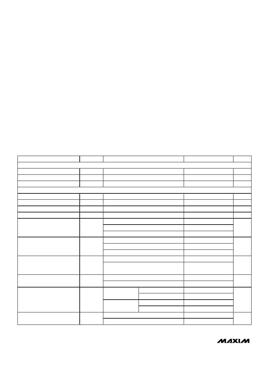
ABSOLUTE MAXIMUM RATINGS
ELECTRICAL CHARACTERISTICS
(VDD = PVDD = 3.3V, PGND = 0V, SHDN = VDD, VCM = 0V, C1 = C2 = 1F, RIN = RF = 5k, RL = ∞, TA = TMIN to TMAX. Typical val-
ues are at TA = +25°C.) (Note 1)
Stresses beyond those listed under “Absolute Maximum Ratings” may cause permanent damage to the device. These are stress ratings only, and functional
operation of the device at these or any other conditions beyond those indicated in the operational sections of the specifications is not implied. Exposure to
absolute maximum rating conditions for extended periods may affect device reliability.
VDD, PVDD to PGND.................................................-0.3V to +6V
VSS, PVSS to PGND ..................................................-6V to +0.3V
IN_ to PGND ..................................(VSS + 0.3V) to (PVDD - 0.3V)
OUT_ to PGND...............................(VSS - 0.3V) to (PVDD + 0.3V)
SHDN to PGND..........................(PGND - 0.3V) to (PVDD + 0.3V)
C1P to PGND.............................(PGND - 0.3V) to (PVDD + 0.3V)
C1N to PGND .............................(PVSS - 0.3V) to (PGND + 0.3V)
Output Short Circuit to PGND or PVDD.......................Continuous
Continuous Power Dissipation (TA = +70°C)
20-Pin QSOP Single-Layer Board
(derate 9.1mW/°C above +70°C) ..................................727mW
20-Pin QSOP Multilayer Board
(derate 11mW/°C above +70°C) ...................................884mW
Operating Temperature Range ...........................-40°C to +85°C
Junction Temperature .....................................................+150°C
Storage Temperature Range .............................-65°C to +150°C
Lead Temperature (soldering, 10s) .................................+300°C
PARAMETER
SYMBOL
CONDITIONS
MIN
TYP
MAX
UNITS
GENERAL
Supply Voltage Range
VDD
Inferred from PSRR test
2.7
5.5
V
Quiescent Current
IDD
Current into VDD and PVDD
12
14
mA
Shutdown Current
IDD, SHDN
VSHDN = 0V
0.1
10
A
AMPLIFIERS
Input Offset Voltage
VOS
±0.5
±5
mV
Input Bias Current
IBIAS
1000
nA
Input Offset Current
IOS
500
nA
Open-Loop Gain
AV
VOUT = -3V to +3V, RL = 1k
82
dB
VDD = 2.7V
-1.6
+1.6
VDD = 3V
-2.3
+2.3
Input Common-Mode Voltage
Range
CMR
VDD = 5V
-3.5
+3.5
V
VDD = 2.7V, VCM = ±1.6V
80
100
VDD = 3V, VCM = ±1.9V
80
100
Common-Mode Rejection Ratio
CMRR
VDD = 5V, VCM = ±3.5V
80
100
dB
VDD = PVDD = 2.7V to 5.5V
80
100
Power-Supply Rejection Ratio
PSRR
f = 1kHz, VDD = PVDD = 5V + 100mVP-P
ripple
60
dB
RL = 1k
, VDD = 3.3V, THD+N = 1%
1.6
2.0
Output Voltage
RL = 1k
, VDD = 5V, THD+N = 1%
2.0
3.0
VRMS
Positive
2.6
3.0
RL = 1k
,
VDD = 3.3V
Negative
-2.6
-3.0
Positive
3.5
4.2
Output Voltage Swing
VOUT
RL = 1k
,
VDD = 5V
Negative
-3.5
-4.1
V
Sinking
40
Output Short-Circuit Current
ISC
Sourcing
5
mA
相关PDF资料 |
PDF描述 |
|---|---|
| MAX9728AETC+T | IC AMP AUDIO .06W STER AB 12TQFN |
| MAX9729ETI+T | IC AMP AUDIO .052W STER 28TQFN |
| MAX9730ETI+T | IC AMP AUDIO PWR 2.4W G 28TQFN |
| MAX9736AETJ/V+ | IC AMP MONO/STER CLASS D 32TQFN |
| MAX9737ETG+T | IC AMP AUDIO 13W MONO D 24TQFN |
相关代理商/技术参数 |
参数描述 |
|---|---|
| MAX9728AETC+ | 功能描述:音频放大器 60mW DirectDrive Headphone Amplifier RoHS:否 制造商:STMicroelectronics 产品:General Purpose Audio Amplifiers 输出类型:Digital 输出功率: THD + 噪声: 工作电源电压:3.3 V 电源电流: 最大功率耗散: 最大工作温度: 安装风格:SMD/SMT 封装 / 箱体:TQFP-64 封装:Reel |
| MAX9728AETC+T | 功能描述:音频放大器 60mW DirectDrive Headphone Amplifier RoHS:否 制造商:STMicroelectronics 产品:General Purpose Audio Amplifiers 输出类型:Digital 输出功率: THD + 噪声: 工作电源电压:3.3 V 电源电流: 最大功率耗散: 最大工作温度: 安装风格:SMD/SMT 封装 / 箱体:TQFP-64 封装:Reel |
| MAX9728AETC+TG104 | 制造商:Maxim Integrated Products 功能描述: |
| MAX9728AETC+TGA8 | 制造商:Maxim Integrated Products 功能描述: |
| MAX9728AEUD+ | 功能描述:音频放大器 60mW DirectDrive Headphone Amplifier RoHS:否 制造商:STMicroelectronics 产品:General Purpose Audio Amplifiers 输出类型:Digital 输出功率: THD + 噪声: 工作电源电压:3.3 V 电源电流: 最大功率耗散: 最大工作温度: 安装风格:SMD/SMT 封装 / 箱体:TQFP-64 封装:Reel |
发布紧急采购,3分钟左右您将得到回复。