- 您现在的位置:买卖IC网 > PDF目录16785 > MAX9737EVKIT+ (Maxim Integrated Products)KIT EVAL FOR MAX9737 PDF资料下载
参数资料
| 型号: | MAX9737EVKIT+ |
| 厂商: | Maxim Integrated Products |
| 文件页数: | 6/13页 |
| 文件大小: | 0K |
| 描述: | KIT EVAL FOR MAX9737 |
| 产品培训模块: | Lead (SnPb) Finish for COTS Obsolescence Mitigation Program |
| 标准包装: | 1 |
| 放大器类型: | D 类 |
| 输出类型: | 1-通道(单声道) |
| 在某负载时最大输出功率 x 通道数量: | 13W x 1 @ 4 欧姆 |
| 电源电压: | 8 V ~ 28 V |
| 工作温度: | -40°C ~ 85°C |
| 板类型: | 完全填充 |
| 已用 IC / 零件: | MAX9737 |
| 已供物品: | 板 |
MAX9737
Mono 7W Class D Amplifier
2
_______________________________________________________________________________________
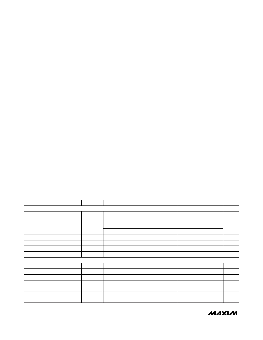
ABSOLUTE MAXIMUM RATINGS
ELECTRICAL CHARACTERISTICS
(VPVDD = 12V, VAGND = VPGND = 0, VSHDN = VMUTE = 5V, C1 = 0.1F, CIN = 0.47F, C2 = CCOM = CREG = 1F, RIN = RFB = 20k
Ω,
RL =
∞, AC measurement bandwidth 22Hz to 22kHz, TA = TMIN to TMAX, unless otherwise noted. Typical values are at TA = +25°C.)
(Note 3)
Stresses beyond those listed under “Absolute Maximum Ratings” may cause permanent damage to the device. These are stress ratings only, and functional
operation of the device at these or any other conditions beyond those indicated in the operational sections of the specifications is not implied. Exposure to
absolute maximum rating conditions for extended periods may affect device reliability.
PVDD to PGND.......................................................-0.3V to +30V
AGND to PGND .....................................................-0.3V to +0.3V
IN, PRE, PC, COM to AGND.....................-0.3V to (VREG + 0.3V)
MUTE, SHDN to AGND ............................................-0.3V to +6V
REG to AGND ...............................................-0.3V to (VS + 0.3V)
VS to AGND ..............................................................-0.3V to +6V
OUT+, OUT- to PGND .............................-0.3V to (PVDD + 0.3V)
C1N to PGND ..........................................-0.3V to (PVDD + 0.3V)
C1P to PGND .........................(PVDD - 0.3V) to (VCHOLD + 0.3V)
CHOLD to PGND .......................................(VC1P - 0.3V) to +36V
OUT+, OUT-, Short Circuit to PGND or PVDD ...........Continuous
Thermal Limits (Notes 1, 2)
Continuous Power Dissipation (TA = +70°C)
24-Pin TQFN Single-Layer PCB (derate 20.8mW/°C
above +70°C)........................................................1666.7mW
θJA................................................................................48°C/W
θJC..................................................................................3°C/W
Continuous Power Dissipation
24-Pin TQFN Multiple-Layer PCB
(derate 27.8mW/°C above +70°C) ........................2222.2mW
θJA................................................................................36°C/W
θJC..................................................................................3°C/W
Operating Temperature Range ...........................-40°C to +85°C
Storage Temperature Range .............................-65°C to +150°C
Junction Temperature ......................................................+150°C
Lead Temperature (soldering, 10s) .................................+300°C
PARAMETER
SYMBOL
CONDITIONS
MIN
TYP
MAX
UNITS
AMPLIFIER DC CHARACTERISTICS
Speaker-Supply Voltage Range
PVDD
Inferred from PSRR test
8
28
V
Undervoltage Lockout
UVLO
6.8
V
TA = +25°C
15
20
Quiescent Supply Current
IPVDD
25
mA
Shutdown Supply Current
ISHDN
VSHDN = 0, TA = +25°C
1
10
A
REG Voltage
VREG
4.0
4.2
4.5
V
Preregulator Voltage
VS
4.85
V
COM Voltage
VCOM
1.94
2.06
2.16
V
INPUT AMPLIFIER CHARACTERISTICS
Capacitive Drive
CL
No sustained oscillation
30
pF
Output Swing
Sinking ±1mA (Note 4)
2.05
V
Open-Loop Gain
AVO
88
dB
Input Offset Voltage
VOS
IN to COM
±2
mV
Input Amplifier Slew Rate
2.5
V/s
Input Amplifier Unity-Gain
Bandwidth
3.5
MHz
Note 1: Thermal performance of this device is highly dependent on PCB layout. See the
Applications Information section for more detail.
Note 2: Package thermal resistances were obtained using the method described in JEDEC specification JESD51-7, using a four-layer
board. For detailed information on package thermal considerations, refer to www.maxim-ic.com/thermal-tutorial.
相关PDF资料 |
PDF描述 |
|---|---|
| H3BBS-2606G | IDC CABLE - HSR26S/AE26G/HSR26S |
| RNF-100-3/32-BN-STK | HEAT SHRINK TUBING |
| V300C15T75B3 | CONVERTER MOD DC/DC 15V 75W |
| 202G632-55-0 | BOOT MOLDED STRAIGHT |
| MC1403BDR2G | IC VREF SERIES PREC 2.5V 8-SOICN |
相关代理商/技术参数 |
参数描述 |
|---|---|
| MAX9737EVKIT+ | 功能描述:音频 IC 开发工具 MAX9737 Eval Kit RoHS:否 制造商:Texas Instruments 产品:Evaluation Kits 类型:Audio Amplifiers 工具用于评估:TAS5614L 工作电源电压:12 V to 38 V |
| MAX9738EVKIT+ | 功能描述:放大器 IC 开发工具 MAX9738 Eval Kit RoHS:否 制造商:International Rectifier 产品:Demonstration Boards 类型:Power Amplifiers 工具用于评估:IR4302 工作电源电压:13 V to 23 V |
| MAX9738EWP+T | 制造商:Maxim Integrated Products 功能描述:16VP-P CLASS G AMPLIFIER WITH INVER - Tape and Reel |
| MAX9738EWP+TG45 | 功能描述:音频放大器 16VP-P Class G Amplifier RoHS:否 制造商:STMicroelectronics 产品:General Purpose Audio Amplifiers 输出类型:Digital 输出功率: THD + 噪声: 工作电源电压:3.3 V 电源电流: 最大功率耗散: 最大工作温度: 安装风格:SMD/SMT 封装 / 箱体:TQFP-64 封装:Reel |
| MAX973C/D | 功能描述:校验器 IC RoHS:否 制造商:STMicroelectronics 产品: 比较器类型: 通道数量: 输出类型:Push-Pull 电源电压-最大:5.5 V 电源电压-最小:1.1 V 补偿电压(最大值):6 mV 电源电流(最大值):1350 nA 响应时间: 最大工作温度:+ 125 C 安装风格:SMD/SMT 封装 / 箱体:SC-70-5 封装:Reel |
发布紧急采购,3分钟左右您将得到回复。