- 您现在的位置:买卖IC网 > PDF目录2091 > MAX9742ETX+ (Maxim Integrated Products)IC AMP AUDIO PWR 20.5W D 36TQFN PDF资料下载
参数资料
| 型号: | MAX9742ETX+ |
| 厂商: | Maxim Integrated Products |
| 文件页数: | 22/36页 |
| 文件大小: | 0K |
| 描述: | IC AMP AUDIO PWR 20.5W D 36TQFN |
| 标准包装: | 50 |
| 类型: | D 类 |
| 输出类型: | 2 通道(立体声) |
| 在某负载时最大输出功率 x 通道数量: | 20.5W x 2 @ 8 欧姆 |
| 电源电压: | 20 V ~ 40 V,±10 V ~ 20 V |
| 特点: | 消除爆音,差分输入,静音,短路和热保护,关机 |
| 安装类型: | 表面贴装 |
| 供应商设备封装: | 36-TQFN 裸露焊盘(6x6) |
| 封装/外壳: | 36-WFQFN 裸露焊盘 |
| 包装: | 管件 |
第1页第2页第3页第4页第5页第6页第7页第8页第9页第10页第11页第12页第13页第14页第15页第16页第17页第18页第19页第20页第21页当前第22页第23页第24页第25页第26页第27页第28页第29页第30页第31页第32页第33页第34页第35页第36页
Supply Bypassing/Layout
To maximize output power and minimize distortion,
proper layout and supply bypassing is essential. To
prevent ground-loop-induced noise and minimize noise
due to parasitic ground inductance, use separate
ground planes for input-signal ground connections
(SGND plane) and output-power ground connections
(PGND plane). For dual-supply applications, connect
MID to the SGND plane. For single-supply operation,
connect MID to an external voltage-divider and bypass
MID to the SGND plane with a decoupling network (see
Figure 11). This provides a sufficient low- and high-fre-
quency AC ground for the internal amplifiers. Connect
the SGND and PGND planes together at a single point
in the PCB near the MAX9742. Minimize the parasitic
trace inductances and resistances associated with the
VDD and VSS connections, by using wide traces of min-
imal length.
Proper power-supply bypassing is essential to ensure
low distortion operation and to prevent excessive sup-
ply pumping when using the single-ended output con-
figuration. For dual-supply operation, bypass VDD and
VSS to PGND with 1000F aluminum electrolytic capac-
itors. VDD and VSS should also be bypassed to PGND
with 0.1F capacitors as physically close as possible to
VDD and VSS pins to provide sufficient high-frequency
decoupling. Also, connect an additional 1F capacitor
between VDD and VSS. For single-supply operation,
bypass VDD to PGND with two 330F capacitors. VDD
should also be bypassed to PGND with an additional
0.1F capacitor as physically close as possible to the
VDD pin.
The MAX9742 includes voltage regulators for the inter-
nal amplifiers, logic circuitry, and gate-drive circuitry
that require external bypassing. Bypass REGP and
REGM to the SGND plane with 1F capacitors. Bypass
REGLS to NSENSE with a 1F capacitor. Bypass LVDD
to LGND with a 0.1F capacitor. The voltage rating
requirements of the external bypass capacitors must
be taken into account. This is especially important
when selecting the REGP and REGM bypass capaci-
tors since the ground-referenced voltages present at
these regulator outputs are dependent on the voltage
applied to the MID input. The minimum required volt-
age ratings for the regulator bypass capacitors are
summarized in Table 4.
Thermal Considerations
Class D amplifiers provide much better efficiency and
thermal performance than a comparable Class AB
amplifier. However, the system’s thermal performance
must be considered with realistic expectations along
with its many parameters.
Continuous Sine Wave vs. Music
When a Class D amplifier is evaluated in the lab, often
a continuous sine wave is used as the signal source.
While this is convenient for measurement purposes, it
represents a worst-case scenario for thermal loading
on the amplifier. It is not uncommon for a Class D
amplifier to enter thermal shutdown if driven near maxi-
mum output power with a continuous sine wave. The
PCB must be optimized for best dissipation (see the
PCB Thermal Considerations section). Audio content,
both music and voice, has a much lower RMS value rel-
ative to its peak output power. Therefore, while an
audio signal may reach similar peaks as a continuous
sine wave, the actual thermal impact on the Class D
amplifier is highly reduced. If the thermal performance
of a system is being evaluated, it is important to use
actual audio signals instead of sine waves for testing. If
sine waves must be used, the thermal performance is
less than the system’s actual capability for real music
or voice.
PCB Thermal Considerations
The exposed paddle is the primary route for conducting
heat away from the IC. With a bottom-side exposed pad-
dle, the PCB and its copper becomes the primary
heatsink for the Class D amplifier. Solder the exposed
paddle to a copper polygon. Add as much copper as
possible from this polygon to any adjacent pin on the
Class D amplifier as well as to any adjacent components,
provided these connections are at the same potential.
MAX9742
Single-/Dual-Supply, Stereo 16W,
Class D Amplifier with Differential Inputs
______________________________________________________________________________________
29
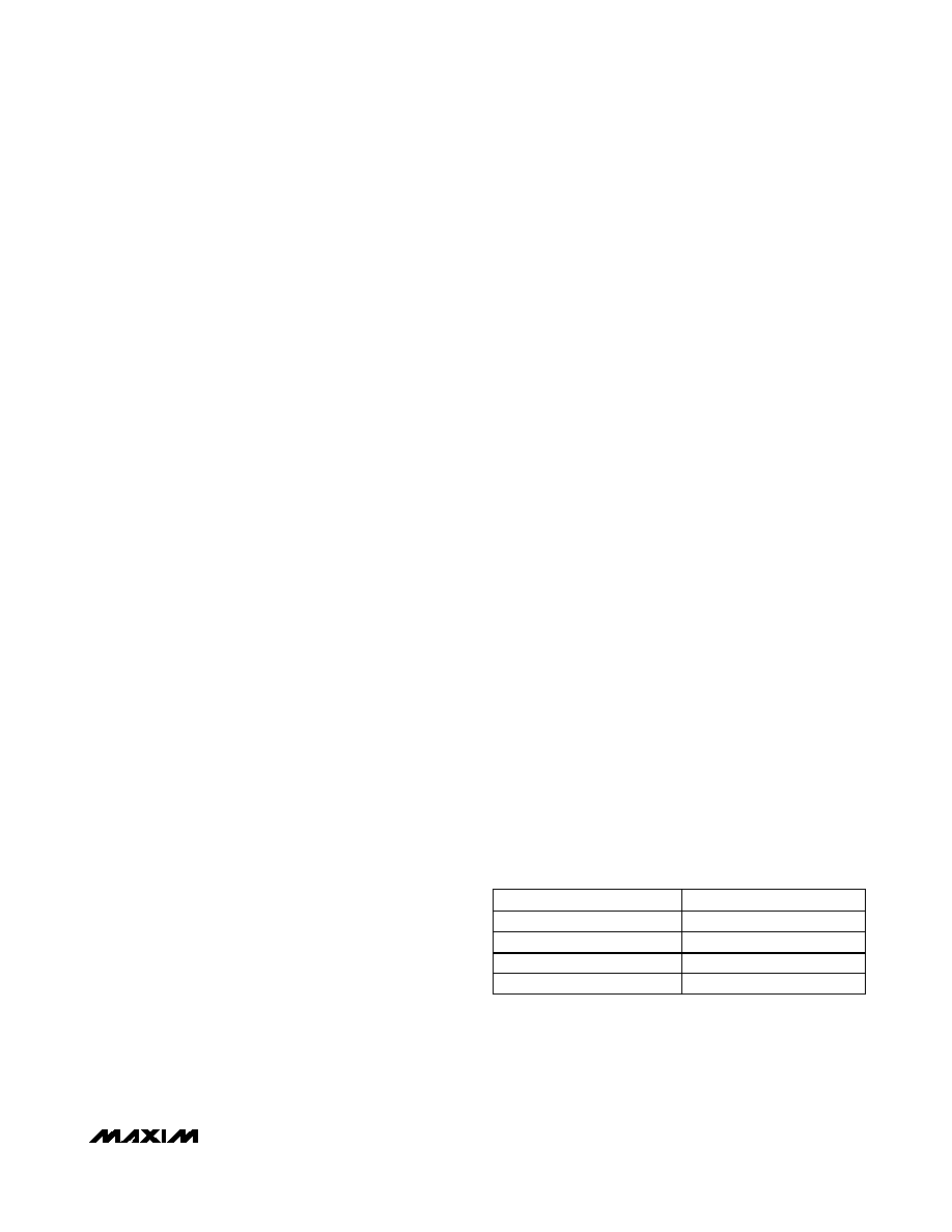
Table 4. Minimum Required Voltage
Ratings for Regulator Bypass Capacitors
CAPACITOR
VOLTAGE RATING (V)
CREGP
VMID + 5
CREGM
VMID - 5
CREGLS
7
CLVDD
5
相关PDF资料 |
PDF描述 |
|---|---|
| MAX9744ETH+ | IC AMP AUDIO PWR 22.5W D 44TQFN |
| MAX9753ETI+T | IC AMP AUDIO PWR 2.2W D 28TQFN |
| MAX9755ETI+T | IC AMP AUDIO PWR 2.6W AB 28TQFN |
| MAX9758ETJ+T | IC AMP AUDIO PWR 2.3W AB 32TQFN |
| MAX9759ETE+T | IC AMP AUDIO PWR 3.2W D 16TQFN |
相关代理商/技术参数 |
参数描述 |
|---|---|
| MAX9742ETX+ | 功能描述:音频放大器 Stereo 16W Class D Amplifier RoHS:否 制造商:STMicroelectronics 产品:General Purpose Audio Amplifiers 输出类型:Digital 输出功率: THD + 噪声: 工作电源电压:3.3 V 电源电流: 最大功率耗散: 最大工作温度: 安装风格:SMD/SMT 封装 / 箱体:TQFP-64 封装:Reel |
| MAX9742ETX+T | 功能描述:音频放大器 Stereo 16W Class D Amplifier RoHS:否 制造商:STMicroelectronics 产品:General Purpose Audio Amplifiers 输出类型:Digital 输出功率: THD + 噪声: 工作电源电压:3.3 V 电源电流: 最大功率耗散: 最大工作温度: 安装风格:SMD/SMT 封装 / 箱体:TQFP-64 封装:Reel |
| MAX9742EVKIT+ | 功能描述:音频放大器 Evaluation Kit for the MAX9742 RoHS:否 制造商:STMicroelectronics 产品:General Purpose Audio Amplifiers 输出类型:Digital 输出功率: THD + 噪声: 工作电源电压:3.3 V 电源电流: 最大功率耗散: 最大工作温度: 安装风格:SMD/SMT 封装 / 箱体:TQFP-64 封装:Reel |
| MAX9744ETH+ | 功能描述:音频放大器 Stereo 20W Class D Amplifier RoHS:否 制造商:STMicroelectronics 产品:General Purpose Audio Amplifiers 输出类型:Digital 输出功率: THD + 噪声: 工作电源电压:3.3 V 电源电流: 最大功率耗散: 最大工作温度: 安装风格:SMD/SMT 封装 / 箱体:TQFP-64 封装:Reel |
| MAX9744ETH+T | 功能描述:音频放大器 Stereo 20W Class D Amplifier RoHS:否 制造商:STMicroelectronics 产品:General Purpose Audio Amplifiers 输出类型:Digital 输出功率: THD + 噪声: 工作电源电压:3.3 V 电源电流: 最大功率耗散: 最大工作温度: 安装风格:SMD/SMT 封装 / 箱体:TQFP-64 封装:Reel |
发布紧急采购,3分钟左右您将得到回复。