- 您现在的位置:买卖IC网 > PDF目录10441 > MAX9788ETI+ (Maxim Integrated Products)IC AMP AUDIO PWR 2.4W G 28TQFN PDF资料下载
参数资料
| 型号: | MAX9788ETI+ |
| 厂商: | Maxim Integrated Products |
| 文件页数: | 6/13页 |
| 文件大小: | 0K |
| 描述: | IC AMP AUDIO PWR 2.4W G 28TQFN |
| 产品培训模块: | Lead (SnPb) Finish for COTS Obsolescence Mitigation Program |
| 标准包装: | 75 |
| 类型: | G 类 |
| 输出类型: | 1-通道(单声道) |
| 在某负载时最大输出功率 x 通道数量: | 2.4W x 1 @ 8 欧姆 |
| 电源电压: | 2.7 V ~ 5.5 V |
| 特点: | 消除爆音,差分输入,关闭 |
| 安装类型: | 表面贴装 |
| 供应商设备封装: | 28-TQFN-EP(5x5) |
| 封装/外壳: | 28-WFQFN 裸露焊盘 |
| 包装: | 管件 |
| 产品目录页面: | 1392 (CN2011-ZH PDF) |
MAX9788
14VP-P, Class G Ceramic Speaker Driver
2
_______________________________________________________________________________________
ABSOLUTE MAXIMUM RATINGS
ELECTRICAL CHARACTERISTICS
(VCC = VCPVDD = VSHDN = 3.6V, VGND = VCPGND = 0V, RIN+ = RIN- = 10k
Ω, RFB+ = RFB- = 10kΩ, RFS = 100kΩ, C1 = 4.7F, C2 =
10F; load connected between OUT+ and OUT-, ZLOAD = 10
Ω + 1F, unless otherwise stated; TA = TMIN to TMAX, unless otherwise
noted. Typical values are at TA = +25°C.) (Notes 2, 3)
Stresses beyond those listed under “Absolute Maximum Ratings” may cause permanent damage to the device. These are stress ratings only, and functional
operation of the device at these or any other conditions beyond those indicated in the operational sections of the specifications is not implied. Exposure to
absolute maximum rating conditions for extended periods may affect device reliability.
(Voltages with respect to GND.)
VCC, CPVDD .............................................................-0.3V to +6V
PVSS, SVSS ...............................................................-6V to +0.3V
CPGND..................................................................-0.3V to +0.3V
OUT+, OUT-...................................(SVSS - 0.3V) to (VCC + 0.3V)
IN+, IN-, FB+, FB- ......................................-0.3V to (VCC + 0.3V)
C1N .........................................(PVSS - 0.3V) to (CPGND + 0.3V)
C1P ......................................(CPGND - 0.3V) to (CPVDD + 0.3V)
FS, SHDN ...................................................-0.3V to (VCC + 0.3V)
Continuous Current Into/Out of
OUT+, OUT-, VCC, GND, SVSS .....................................800mA
CPVDD, CPGND, C1P, C1N, PVSS.................................800mA
Any Other Pin ..................................................................20mA
Continuous Power Dissipation (TA = +70°C)
20-Bump WLP (derate 10.3mW/°C
above +70°C) (Note 1)..................................................827mW
28-Pin TQFN (derate 20.8mW/°C above +70°C) ........1667mW
Operating Temperature Range ...........................-40°C to +85°C
Storage Temperature Range .............................-65°C to +150°C
Lead Temperature (soldering, 10s) ................................+300°C
Bump Temperature (soldering) Reflow............................+235°C
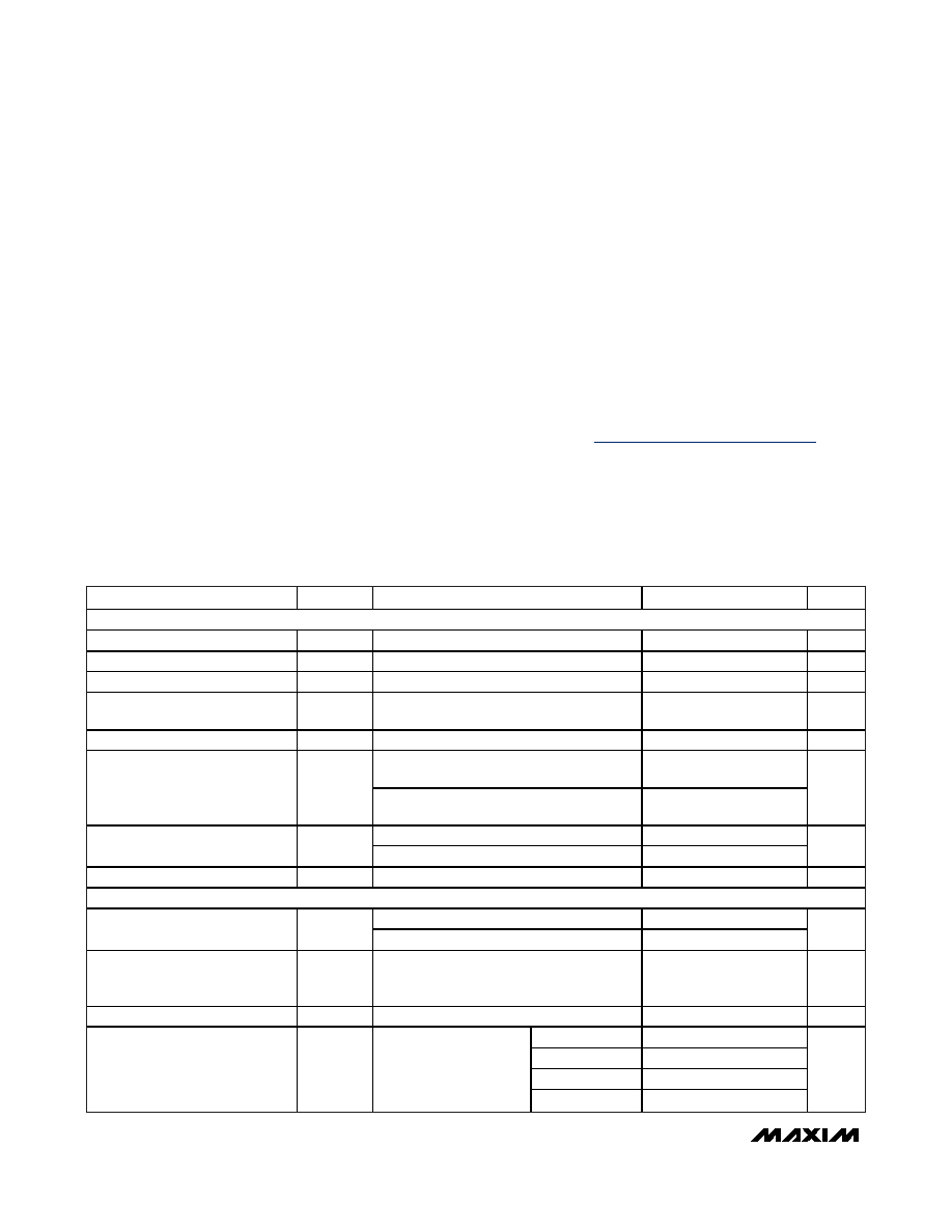
PARAMETER
SYMBOL
CONDITIONS
MIN
TYP
MAX
UNITS
GENERAL
Supply Voltage Range
VCC
Inferred from PSRR test
2.7
5.5
V
Quiescent Current
ICC
812
mA
Shutdown Current
ISHDN
SHDN = GND
0.3
5
A
Turn-On Time
tON
Time from shutdown or power-on to full
operation
50
ms
Input DC Bias Voltage
VBIAS
IN_ inputs (Note 4)
1.1
1.24
1.4
V
ILOAD = 0mA (slow mode)
55
83
110
Charge-Pump Oscillator
Frequency
fOSC
ILOAD > 100mA (normal mode)
230
330
470
kHz
VIH
1.4
SHDN Input Threshold
(Note 5)
VIL
0.4
V
SHDN Input Leakage Current
±1
A
SPEAKER AMPLIFIER
TA = +25°C
±3
±15
Output Offset Voltage
VOS
TMIN
≤ TA ≤ TMAX
±20
mV
Click-and-Pop Level
VCP
Peak voltage into/out of shutdown
A-weighted, 32 samples per second
(Notes 6, 7)
-67
dBV
Voltage Gain
AV
(Notes 4, 8)
11.5
12
12.5
dB
VCC = 5V
7.1
VCC = 4.2V
5.9
VCC = 3.6V
5.1
Output Voltage
VOUT
f = 1kHz, 1% THD+N
VCC = 3.0V
4.2
VRMS
Note 1: Package thermal resistances were obtained using the method described in JEDEC specification JESD51-7, using a four-
layer board. For detailed information on package thermal considerations, see www.maxim-ic.com/thermal-tutorial.
相关PDF资料 |
PDF描述 |
|---|---|
| MAX9730ETI+ | IC AMP AUDIO PWR 2.4W G 28TQFN |
| JMK042BJ222KC-F | CAP CER 2200PF 6.3V X5R 01005 |
| CXC3102A10SL4P | CONN RCPT 2POS PNL MNT PIN |
| VI-BW0-MW | CONVERTER MOD DC/DC 5V 100W |
| VI-B7T-MX-F1 | CONVERTER MOD DC/DC 6.5V 75W |
相关代理商/技术参数 |
参数描述 |
|---|---|
| MAX9788ETI+ | 功能描述:音频放大器 14VP-P Class G Cer Speaker Driver RoHS:否 制造商:STMicroelectronics 产品:General Purpose Audio Amplifiers 输出类型:Digital 输出功率: THD + 噪声: 工作电源电压:3.3 V 电源电流: 最大功率耗散: 最大工作温度: 安装风格:SMD/SMT 封装 / 箱体:TQFP-64 封装:Reel |
| MAX9788ETI+ | 制造商:Maxim Integrated Products 功能描述:IC AUDIO PWR AMP CLASS G 2.4W TQFN-28 |
| MAX9788ETI+T | 功能描述:音频放大器 14VP-P Class G Cer Speaker Driver RoHS:否 制造商:STMicroelectronics 产品:General Purpose Audio Amplifiers 输出类型:Digital 输出功率: THD + 噪声: 工作电源电压:3.3 V 电源电流: 最大功率耗散: 最大工作温度: 安装风格:SMD/SMT 封装 / 箱体:TQFP-64 封装:Reel |
| MAX9788EVKIT+ | 功能描述:音频 IC 开发工具 MAX9788 Eval Kit RoHS:否 制造商:Texas Instruments 产品:Evaluation Kits 类型:Audio Amplifiers 工具用于评估:TAS5614L 工作电源电压:12 V to 38 V |
| MAX9788EWP+TG45 | 功能描述:音频放大器 14VP-P Class G Cer Speaker Driver RoHS:否 制造商:STMicroelectronics 产品:General Purpose Audio Amplifiers 输出类型:Digital 输出功率: THD + 噪声: 工作电源电压:3.3 V 电源电流: 最大功率耗散: 最大工作温度: 安装风格:SMD/SMT 封装 / 箱体:TQFP-64 封装:Reel |
发布紧急采购,3分钟左右您将得到回复。