- 您现在的位置:买卖IC网 > PDF目录10729 > MAX983EPA+ (Maxim Integrated Products)IC COMPARATOR OD 8-DIP PDF资料下载
参数资料
| 型号: | MAX983EPA+ |
| 厂商: | Maxim Integrated Products |
| 文件页数: | 2/17页 |
| 文件大小: | 0K |
| 描述: | IC COMPARATOR OD 8-DIP |
| 产品培训模块: | Lead (SnPb) Finish for COTS Obsolescence Mitigation Program |
| 标准包装: | 50 |
| 类型: | 带电压基准 |
| 元件数: | 2 |
| 输出类型: | 开路漏极 |
| 电压 - 电源,单路/双路(±): | 2.5 V ~ 11 V,±1.25 V ~ 5.5 V |
| 电压 - 输入偏移(最小值): | 10mV @ 5V |
| 电流 - 输出(标准): | 0.015mA @ 5V |
| 电流 - 静态(最大值): | 6µA |
| CMRR, PSRR(标准): | 80dB CMRR,80dB PSRR |
| 磁滞: | 50mV |
| 工作温度: | -40°C ~ 85°C |
| 封装/外壳: | 8-DIP(0.300",7.62mm) |
| 安装类型: | 通孔 |
| 包装: | 管件 |
| 产品目录页面: | 1386 (CN2011-ZH PDF) |
MAX971–MAX974/MAX981–MAX984
Ultra-Low-Power, Open-Drain,
Single/Dual-Supply Comparators
10
______________________________________________________________________________________
Low-Voltage Operation: V+ = 1V
(MAX9_4 Only)
The guaranteed minimum operating voltage is 2.5V (or
±1.25V). As the total supply voltage falls below 2.5V,
performance degrades and the supply current falls. The
reference will not function below about 2.2V, although
the comparators will continue to operate with a total
supply voltage as low as 1V. While the MAX9_4 has
comparators that may be used at supply voltages below
2V, the MAX9_1/MAX9_2/MAX9_3 may not be used with
supply voltages below 2.5V.
At low supply voltages, the comparators’ output sink
capability is reduced and the propagation delay
increases (see Typical Operating Characteristics). The
useful input voltage range extends from the negative
supply to a little under 1V below the positive supply,
which is slightly closer to the positive rail than when the
device operates from higher supply voltages. Test your
prototype over the full temperature and supply-voltage
range if you anticipate operation below 2.5V.
Comparator Output
With 100mV of overdrive, propagation delay is typically
3s. The Typical Operating Characteristics show the
propagation delay for various overdrive levels. The
open-drain outputs are intended for wire-ORed and
level-shifting applications. The maximum output voltage
is 11V above V-, and may be applied even when no
supply voltage is present (V+ = V-).
The MAX9_1 and MAX9_4 outputs sink current to GND,
making these devices ideal for bipolar to single-ended
conversion and level-shifting applications.
The negative supply does not affect the output sink
current. The positive supply provides gate drive for the
output N-channel MOSFET and heavily influences the
output current capability, especially at low supply
voltages (see Typical Operating Characteristics section).
The MAX9_2 and MAX9_3 have no GND pin, and their
outputs sink current to V-.
Voltage Reference
The internal bandgap voltage reference has an output
of 1.182V above V-. Note that the REF voltage is
referenced to V-, not to GND. Its accuracy is ±1%
(MAX971/MAX973/MAX974) or ±2% (MAX981–MAX984)
in the 0°C to +70°C range. The REF output is typically
capable of sourcing 25A and sinking 15A. Do not
bypass the REF output.
Noise Considerations
Although the comparators have a very high gain, useful
gain is limited by noise. This is shown in the Transfer
Function graph (see Typical Operating Characteristics).
As the input voltage approaches the comparator’s
offset, the output begins to bounce back and forth; this
peaks when VIN = VOS. (The lowpass filter shown on the
graph averages out the bouncing, making the transfer
function easy to observe.) Consequently, the
comparator has an effective wideband peak-to-peak
noise of around 300V. The voltage reference has
peak-to-peak noise approaching 1mV. Thus, when a
comparator is used with the reference, the combined
peak-to-peak noise is about 1mV. This, of course, is
much higher than the RMS noise of the individual
components. Take care in your layout to avoid
capacitive coupling from any output to the reference
pin. Crosstalk can significantly increase the actual
noise of the reference.
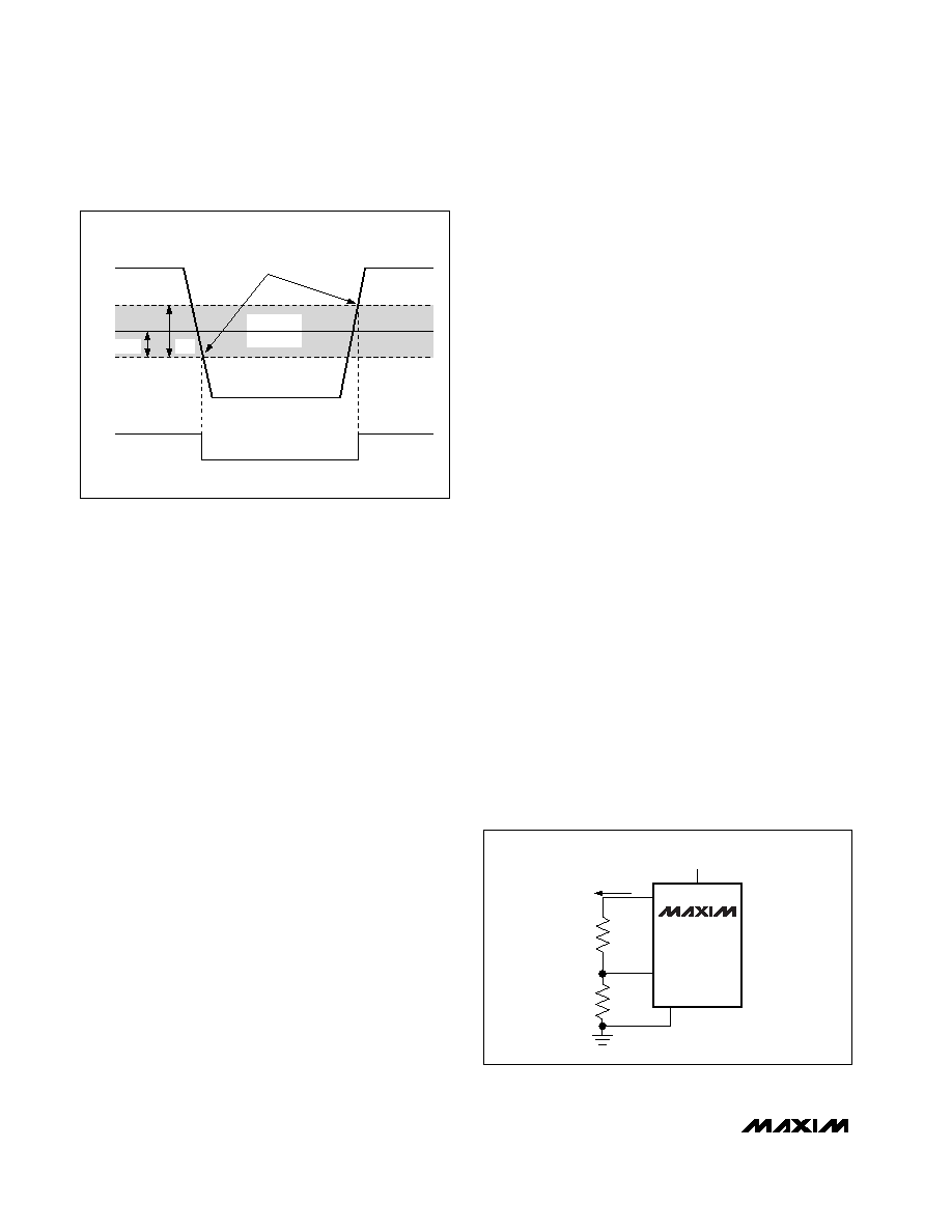
THRESHOLDS
OUT
IN-
IN+
VHB
HYSTERESIS
BAND
VREF - VHYST
Figure 2. Threshold Hysteresis Band
7
2
5
6
HYST
REF
V-
V+
R1
R2
MAX9_1
MAX982
MAX9_3
2.5V TO 11V
IREF
Figure 3. Programming the HYST Pin
相关PDF资料 |
PDF描述 |
|---|---|
| MAX942CPA+ | IC COMPARATOR R-R 8-DIP |
| MAX918ESA+ | IC COMPARATOR BTR 8-SOIC |
| MAX516ACWG+ | IC COMP QUAD PROGR THRES 24-SOIC |
| VE-254-MY-B1 | CONVERTER MOD DC/DC 48V 50W |
| VE-JNB-MY-F3 | CONVERTER MOD DC/DC 95V 50W |
相关代理商/技术参数 |
参数描述 |
|---|---|
| MAX983EPA+ | 功能描述:校验器 IC Dual Comparator / Reference RoHS:否 制造商:STMicroelectronics 产品: 比较器类型: 通道数量: 输出类型:Push-Pull 电源电压-最大:5.5 V 电源电压-最小:1.1 V 补偿电压(最大值):6 mV 电源电流(最大值):1350 nA 响应时间: 最大工作温度:+ 125 C 安装风格:SMD/SMT 封装 / 箱体:SC-70-5 封装:Reel |
| MAX983ESA | 功能描述:校验器 IC Dual Comparator / Reference RoHS:否 制造商:STMicroelectronics 产品: 比较器类型: 通道数量: 输出类型:Push-Pull 电源电压-最大:5.5 V 电源电压-最小:1.1 V 补偿电压(最大值):6 mV 电源电流(最大值):1350 nA 响应时间: 最大工作温度:+ 125 C 安装风格:SMD/SMT 封装 / 箱体:SC-70-5 封装:Reel |
| MAX983ESA+ | 功能描述:校验器 IC Dual Comparator / Reference RoHS:否 制造商:STMicroelectronics 产品: 比较器类型: 通道数量: 输出类型:Push-Pull 电源电压-最大:5.5 V 电源电压-最小:1.1 V 补偿电压(最大值):6 mV 电源电流(最大值):1350 nA 响应时间: 最大工作温度:+ 125 C 安装风格:SMD/SMT 封装 / 箱体:SC-70-5 封装:Reel |
| MAX983ESA+T | 功能描述:校验器 IC Dual Comparator / Reference RoHS:否 制造商:STMicroelectronics 产品: 比较器类型: 通道数量: 输出类型:Push-Pull 电源电压-最大:5.5 V 电源电压-最小:1.1 V 补偿电压(最大值):6 mV 电源电流(最大值):1350 nA 响应时间: 最大工作温度:+ 125 C 安装风格:SMD/SMT 封装 / 箱体:SC-70-5 封装:Reel |
| MAX983ESA-T | 功能描述:校验器 IC Dual Comparator / Reference RoHS:否 制造商:STMicroelectronics 产品: 比较器类型: 通道数量: 输出类型:Push-Pull 电源电压-最大:5.5 V 电源电压-最小:1.1 V 补偿电压(最大值):6 mV 电源电流(最大值):1350 nA 响应时间: 最大工作温度:+ 125 C 安装风格:SMD/SMT 封装 / 箱体:SC-70-5 封装:Reel |
发布紧急采购,3分钟左右您将得到回复。